

Parallel Signal Via Structure
a parallel signal and via technology, applied in the field of thrusilicon vias, to achieve the effect of reducing any difference in propagation delay
- Summary
- Abstract
- Description
- Claims
- Application Information
AI Technical Summary
Benefits of technology
Problems solved by technology
Method used
Image

Examples
Embodiment Construction
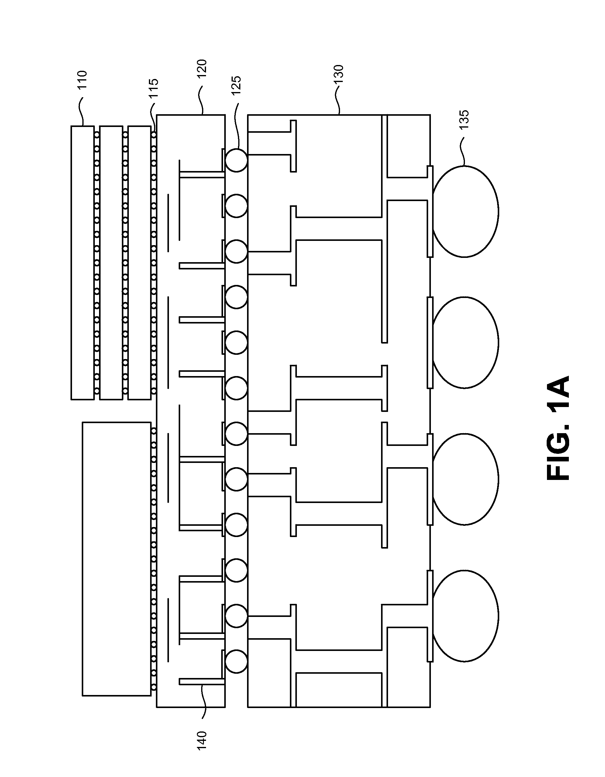
[0022]FIG. 1A is a cross sectional side view of a three dimensional (3D) and 2.5D integrated circuit (3DIC). A 3DIC typically includes a stack of alternating active chips and silicon interposers. As shown in FIG. 1, an exemplary 3DIC may include several tiles 110 (e.g., logic, field programmable gate arrays or FPGA, memory-stacks, integrated passive devices or IPD, etc), a passive silicon interposer 120 and an organic laminate 130. In order to route signals, one or more of these components may include thru-silicon vias (TSV).
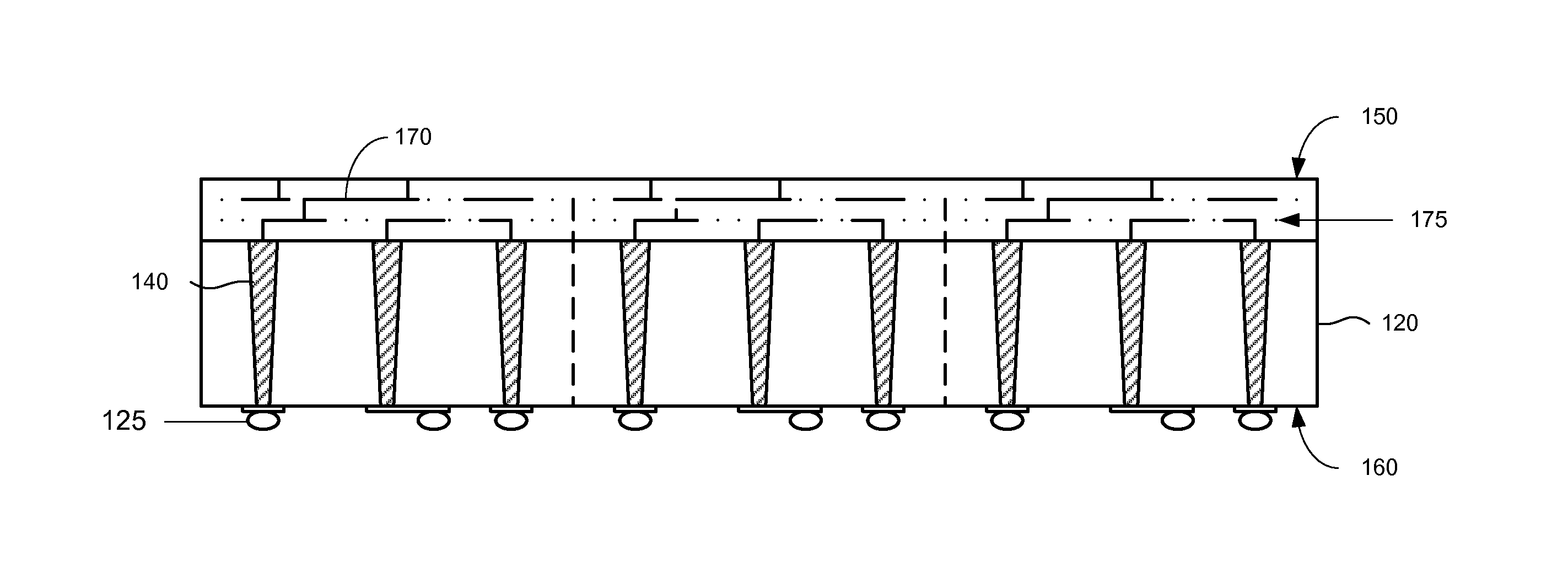
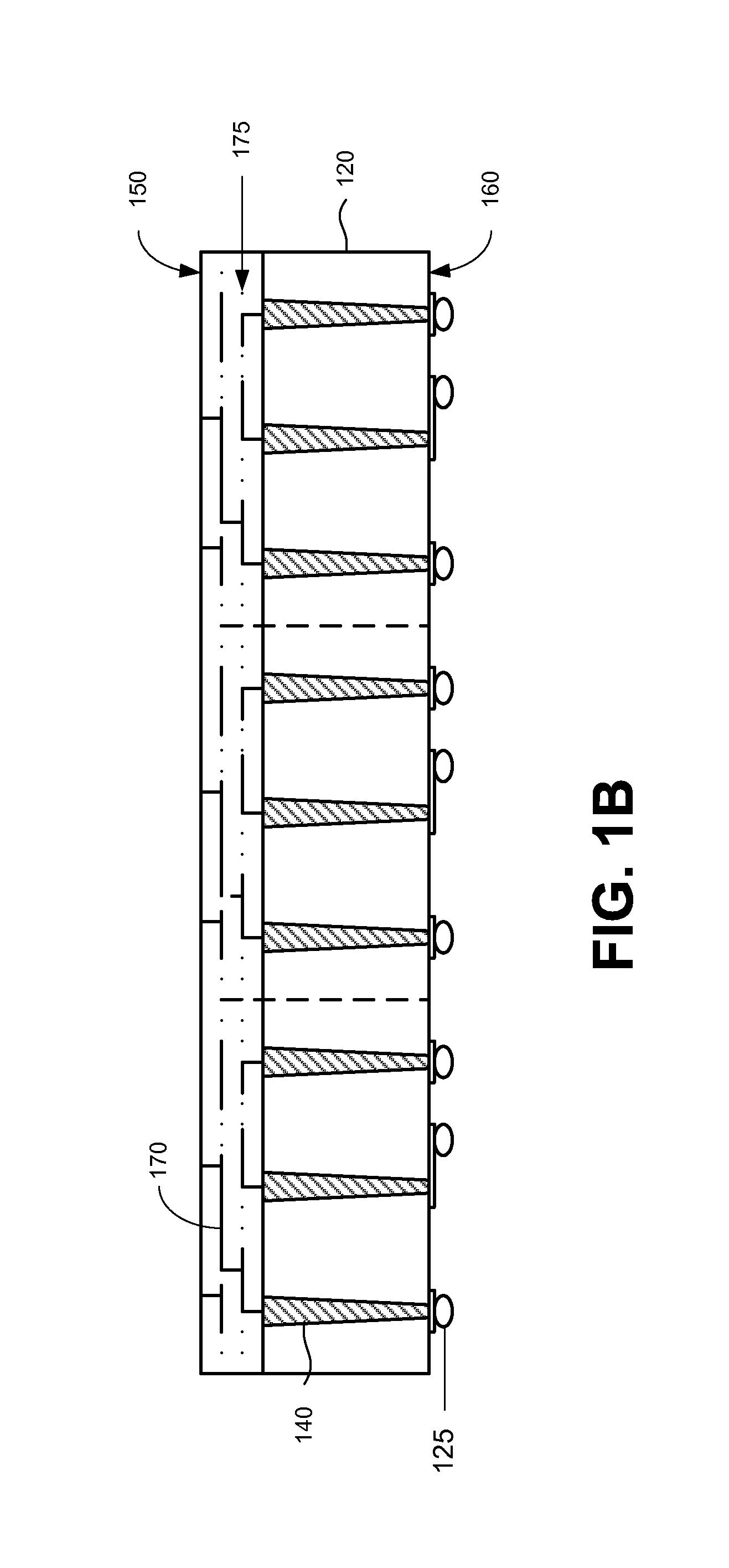
[0023]FIG. 1B is a cross sectional side view of a silicon interposer 120, according to one embodiment of the invention. Silicon interposer 120 may route signals from a one side 150 of the interposer to the other side 160 of the interposer. For instance, the first side 150 may be used to interface to an integrated circuit, and the second side 160 may be used to interface to an organic laminate or a printed circuit board. Silicon interposer 120 may also route sign...
PUM
 Abstract
Description
Claims
Application Information