Semiconductor package device and method of manufacturing the same

a technology of semiconductor and package device, which is applied in the direction of semiconductor device, semiconductor/solid-state device details, electrical apparatus, etc., can solve the problem of taking a great cost to use the tsv interposer to provide electrical interconnection between the two dies

Active Publication Date: 2018-11-22
ADVANCED SEMICON ENG INC
View PDF1 Cites 9 Cited by
  • Summary
  • Abstract
  • Description
  • Claims
  • Application Information

AI Technical Summary

Problems solved by technology

However, it may take great cost to use the TSV interposer to provide electrical interconnection between the two dies.

Method used


Image

  • Semiconductor package device and method of manufacturing the same
  • Semiconductor package device and method of manufacturing the same
  • Semiconductor package device and method of manufacturing the same

Examples


Embodiment Construction

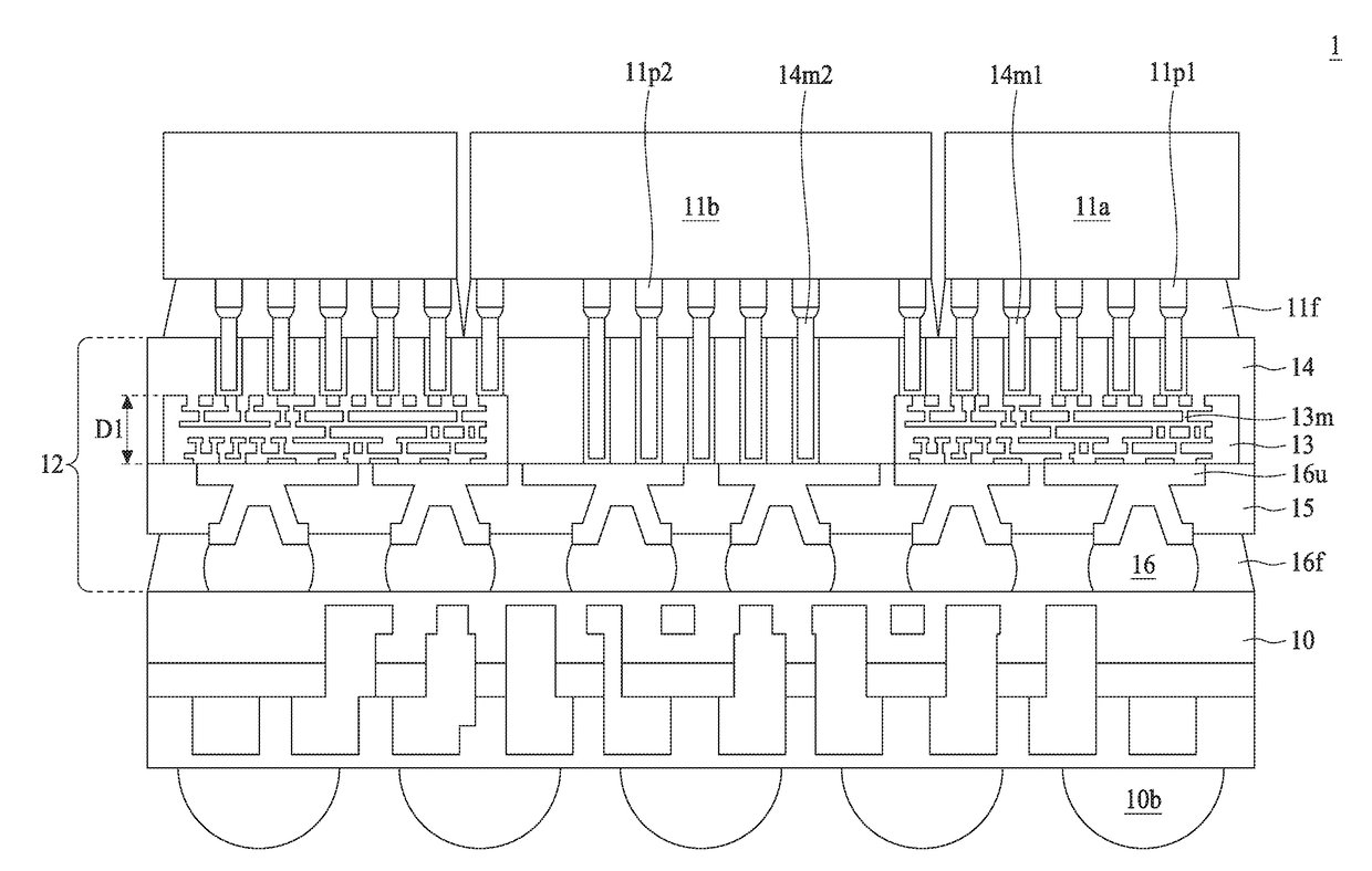
[0012]FIG. 1 illustrates a cross-sectional view of a semiconductor package device 1 in accordance with some embodiments of the present disclosure. The semiconductor package device 1 includes a substrate 10, electronic components 11a, 11b and an interconnection component 12.

[0013]The substrate 10 may be a flexible substrate or a rigid substrate, depending upon the specific application. In some embodiments, the substrate 10 includes a plurality of electrical traces disposed therein. In some embodiments, an external contact layer is also formed or disposed on the substrate 10. In some embodiments, the external contact layer includes a ball grid array (BGA). In other embodiments, the external contact layer includes an array such as, but not limited to, a land grid array (LGA) or an array of pins (PGA). In some embodiments, the external contact layer includes solder balls 10b, which are used and are composed of lead or are lead free (e.g., including such materials as alloys of gold and t...


PUM


Abstract

A semiconductor package device includes a first interconnection structure, a non-silicon interposer and a first die. The first interconnection structure has a first pitch. The non-silicon interposer surrounds the first interconnection structure. The non-silicon interposer includes a second interconnection structure having a second pitch. The second pitch is larger than the first pitch. The first die is above the first interconnection structure and is electrically connected to the first interconnection structure.

Description

BACKGROUND1. Technical Field[0001]The present disclosure relates generally to a semiconductor package device and a method of manufacturing the same. More particularly, the present disclosure relates to a semiconductor package device including a stacking structure and a method of manufacturing the same.2. Description of the Related Art[0002]In comparable three-dimensional semiconductor packages, there is a bridge in an interposer (e.g., a through silicon via (TSV) interposer) to provide electrical interconnection (e.g., via a redistribution layer (RDL)) between two dies (such as an application-specific integrated circuit (ASIC) and a high bandwidth memory (HBM)). However, fine pitch (e.g., smaller than 1 micrometer (μm)) interconnection exists in a small portion of the interposer (e.g., the area between the two dies). Most of the regions of the interposer are designed for interconnection with relatively great pitch (e.g., greater than 1 μm). However, it may take great cost to use the...

Claims


Application Information

Patent Timeline
Patent Type & Authority Applications(United States)
IPC IPC(8): H01L23/538H01L21/48H01L23/498H01L21/683
CPCH01L23/49838H01L23/49827H01L21/486H01L21/6835H01L2221/68345H01L23/49822H01L23/5384H01L21/4857H01L23/5383H01L23/49816H01L2221/68359H01L21/4846H01L24/81H01L2224/02379H01L2224/02331H01L2224/812H01L2224/16225H01L2224/18H01L23/3128H01L21/56H01L23/5385
Inventor CHANG CHIEN, CHIEN LINKAO, CHIN-LIWANG, SHIH-YULEE, CHANG CHI
Owner ADVANCED SEMICON ENG INC
Why Eureka
Try Eureka