Light emitting device and electrical appliance

a technology of light emitting devices and electrical appliances, applied in the direction of static indicating devices, thermoelectric devices, instruments, etc., can solve the problems of short luminous time per pixel, the theoretical upper limit of luminous efficiency has always been a problem, and the driving principle of a passive matrix type light emitting device becomes a problem

Inactive Publication Date: 2004-01-13
SEMICON ENERGY LAB CO LTD
View PDF14 Cites 102 Cited by
  • Summary
  • Abstract
  • Description
  • Claims
  • Application Information

AI Technical Summary

Benefits of technology

Another object of the present invention is to provide an electrical appliance which has a bright display portion and low electric power consumption, by using the light emitting device.
Still another object of the present invention is to provide an electrical appliance having low electric power consumption by using the light emitting device of the present invention as a light source (typically, a backlight).

Problems solved by technology

Although various kinds of luminescent materials from a low molecular material to a high molecular material are developed, a theoretical upper limit of luminous efficiency has been always a problem.
Here, the driving principle of a passive matrix type light emitting device becomes a problem.
That is, as the number of pixels becomes large and the fineness becomes high, a luminous time per pixel becomes short.
Accordingly, in order to obtain high luminous brightness, it is necessary that a higher current is made to flow, and as a result, the electric power consumption increases and the EL film is deteriorated.

Method used


Image

  • Light emitting device and electrical appliance
  • Light emitting device and electrical appliance
  • Light emitting device and electrical appliance

Examples


embodiment 1

In this embodiment, an example of an active matrix type light emitting device using a triplet EL component is described referring to FIG. 15. The active matrix type light emitting device shown in FIG. 15 is formed with a pixel portion 585 and a driver circuit 584 which outputs a signal to the pixel portion. In the pixel portion 585 there are provided a switching FT 582 and a driver TFT 583, and in the driver circuit there are provided a p-channel TFT 580 and an n-channel TFT 581.

In the pixel portion 585, the semiconductor layer of the switching TFT 582 has as an n-type impurity region a source region 560 and drain regions 561 and 568 and LDD regions 562 to 565. This TFT has a multi gate structure and is formed with channel forming regions 566 and 567 by the gate electrode 513 on the gate insulating film 510. Further, LDD regions 562 to 565 are provided in positions that do not overlap with the gate electrode 513, and is a structure which aims to decrease the off-current of the TFT.

T...

embodiment 2

A circuit diagram of the pixel of the active matrix type light emitting device is shown in FIG. 16. Reference numeral 1107 denotes a switching TFT, reference numeral 1108 denotes a driver TFT, reference numeral 1109 denotes an erasure TFT, reference numeral 1110 denotes an EL element, reference numeral 1111 denotes an opposing power source, and reference numeral 1112 is a capacitor. The driver TFT 1108 is one in which two EL driver TFTs (a first EL driver TFT and a second EL driver TFT) are connected in parallel. The first EL driver TFT and the second EL driver TFT are combined and referred to as the driver TFT in this specification.

A gate electrode of the switching TFT 1107 is connected to a write in gate signal line Ga (one of the write in gate signal lines Ga1 to Gay). One of a source region and a drain region of the switching TFT 1107 is connected to a source signal line S (one of the source signal lines S1 to Sx), and the other is connected to a gate electrode of the driver TFT...

embodiment 3

The superiority of the triplet EL element in respect to the singlet EL element is in that a high precision may be obtained with low voltage. Here, a test example of applying the EL element to the active matrix type light emitting device is shown.

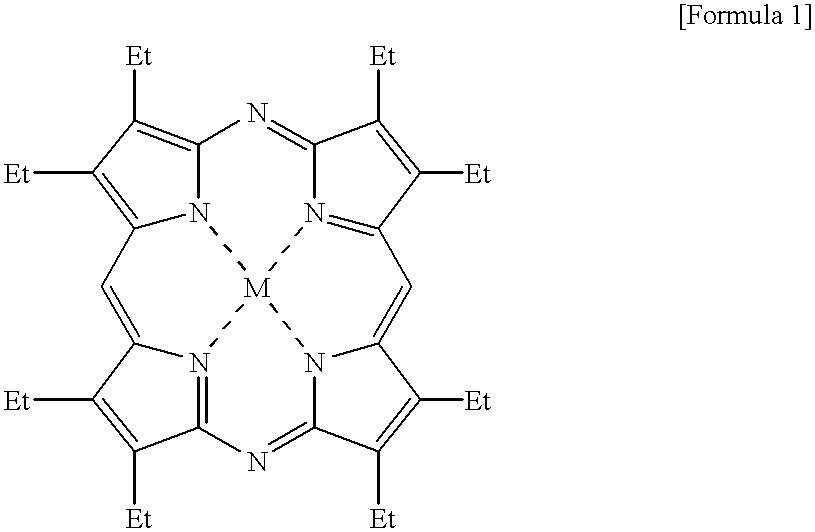
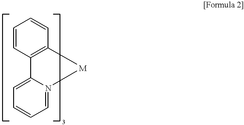
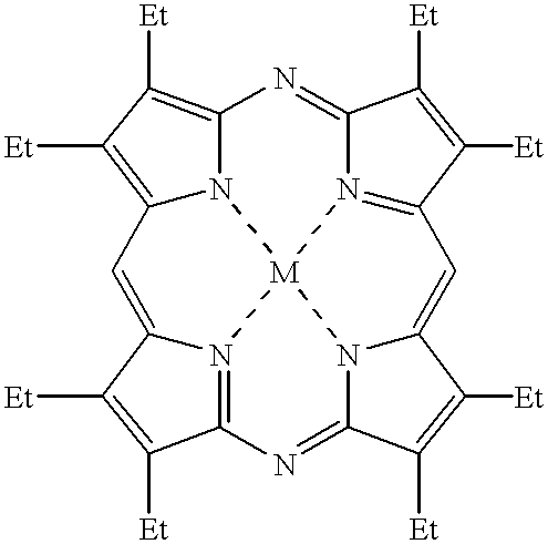
As a triplet EL element and an anode, a copper phthalocyanine (hereinafter referred to as CuPc), 4,4',4"-tris (N-3-methylphenyl-N-phenyl-amino) triphenylamine (hereinafter referred to as mTDATA) which is an aromatic amine material, 4,4'-bis [N-naphthyl-N pheny-amino] biphenyl (hereinafter referred to as .alpha.-NPD), 4,4' N,N'-dicaribazole-biphenyl (hereinafter referred to as CBP) added with tris-(2-phenyl-pyridine and iridium (hereinafter referred to as Ir (ppy).sub.3), bathocuproine (hereinafter referred to as BCP), an aluminum complex of oxine (hereinafter referred to as Alq.sub.3) are laminated subsequently to fabricate the sample. CBP added with Ir (ppy).sub.3 is an organic compound where light emission (fluorescence) may be obtained fr...


PUM


Abstract

There is provided a light emitting device which is bright and has low electric power consumption and high reliability. A triplet EL element 203 electrically connected to a current controlling TFT 102 is provided in a pixel portion 201. A luminescent material used for the triplet EL element 203 has a feature that EL is obtained by triplet excitation, and exhibits high luminous efficiency at a low operation voltage as compared with the prior art. Accordingly, the operation is made at the low operation voltage, so that the light emitting device which is bright and has low electric power consumption and high reliability can be obtained.

Description

1. Field of the InventionThe present invention relates to a light emitting device including a element (hereinafter referred to as an EL element) in which a thin film (hereinafter referred to as an EL film) made of a luminescent material capable of generating electroluminescence (hereinafter abbreviated as EL) is interposed between a pair of electrodes. Incidentally, in the present specification, an EL element using a luminescent material in which EL is obtained by singlet excitation is called a singlet EL element, and an EL element using a luminescent material in which EL is obtained by triplet excitation is called a triplet EL element.2. Description of the Related ArtIn recent years, an EL element using an organic EL film as a light emitting layer has been developed, and EL elements using various organic EL films have been proposed. An attempt to realize a flat panel display by employing a light emitting device, which uses an EL element of the kind as a light emitting element, has ...

Claims


Application Information

Patent Timeline
Patent Type & Authority Patents(United States)
IPC IPC(8): H01L51/50H01L51/30H01L51/05H01L27/32H01L27/28G09G3/20G09G3/32G09G3/36H01L51/00
CPCH01L27/3244H01L51/0077H01L51/0084H01L51/5016G09G3/2022G09G3/3258G09G3/3607G09G2300/0426G09G2300/0842G09G2310/0251H01H2219/037H01L27/1214H01L51/0078H01L51/0081H10K59/12H10K85/311H10K85/30H10K85/324H10K85/341H10K50/11H10K2101/10
Inventor YAMAZAKI, SHUNPEIINUKAI, KAZUTAKA
Owner SEMICON ENERGY LAB CO LTD
Why Eureka
Try Eureka