Uniformly doped source/drain junction in a double-gate MOSFET

a source/drain junction and mosfet technology, applied in the direction of semiconductor devices, electrical equipment, transistors, etc., can solve the problem that conventional mosfets have difficulty scaling below 50 nm fabrication processing

Inactive Publication Date: 2004-04-06
ADVANCED MICRO DEVICES INC
View PDF12 Cites 134 Cited by
  • Summary
  • Abstract
  • Description
  • Claims
  • Application Information

AI Technical Summary

Problems solved by technology

Conventional MOSFETs have difficulty scaling below 50 nm fabrication processing.

Method used


Image

  • Uniformly doped source/drain junction in a double-gate MOSFET
  • Uniformly doped source/drain junction in a double-gate MOSFET
  • Uniformly doped source/drain junction in a double-gate MOSFET

Examples


Embodiment Construction

refers to the accompanying drawings. The same reference numbers may be used in different drawings to identify the same or similar elements. Also, the following detailed description does not limit the invention. Instead, the scope of the invention is defined by the appended claims and equivalents.

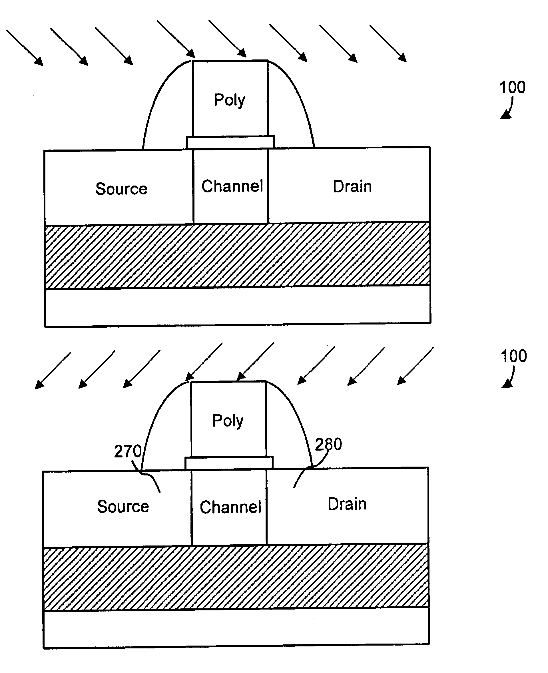
A FinFET is described that has a relatively uniform dopant concentration in the source / drain junction. The uniform dopant concentration is achieved through multiple tilted implantations. The uniform dopant concentration can be advantageous as it may provide for uniform channel length along the width and better short channel control.

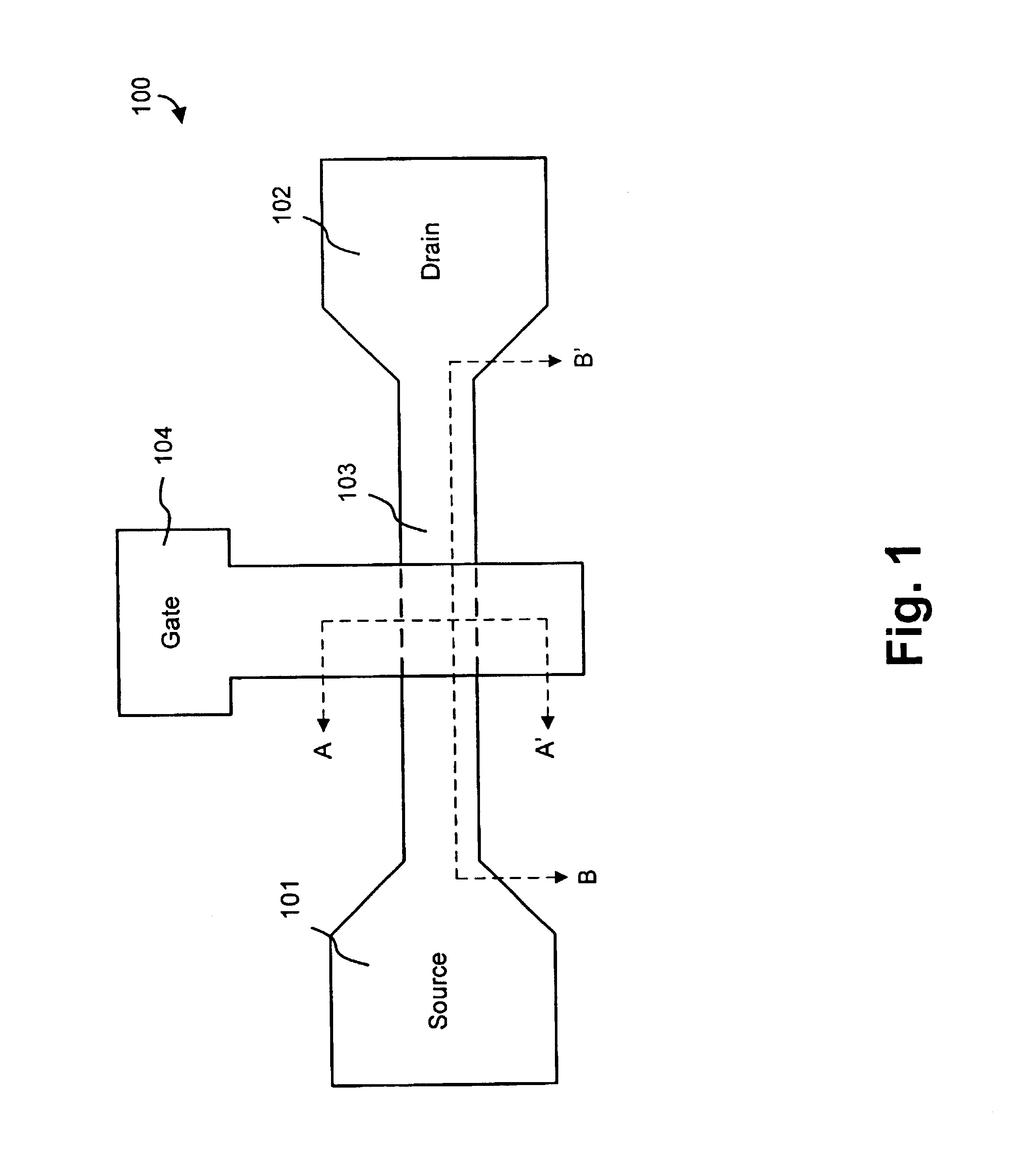
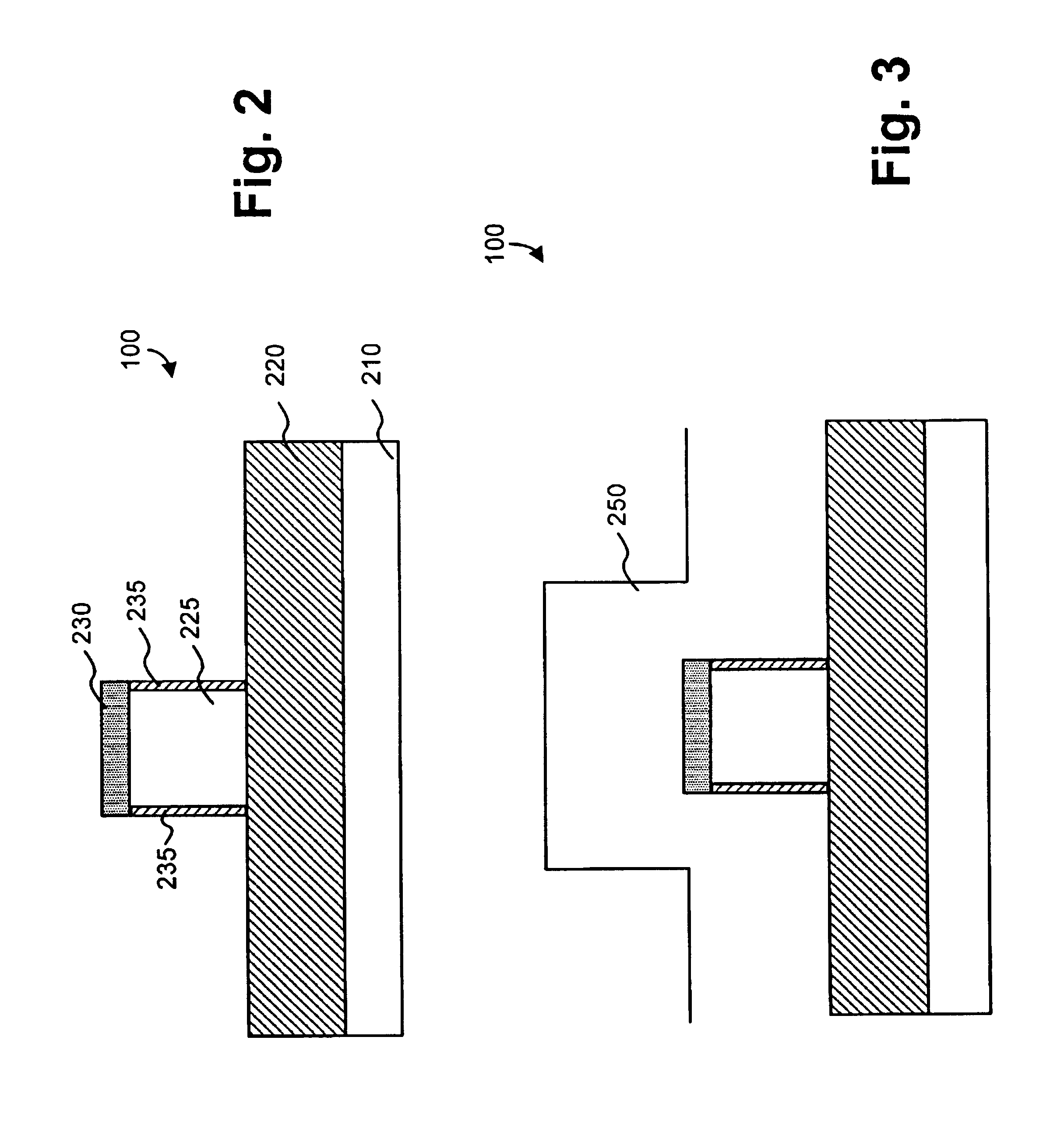
FIG. 1 is a top-level view of a FinFET 100 consistent with principles of the invention. FinFET 100 includes a source region 101, a drain region 102, a gate 104, and a fin 103. The portion of fin 103 that is under gate 104 is the channel for the transistor. FIGS. 2 and 3 are cross-sectional views taken along the line A-A' in FIG. 1. FIGS. 5-8 are cross-sectional vi...


PUM


Abstract

Multiple dopant implantations are performed on a FinFET device to thereby distribute the dopant in a substantially uniform manner along a vertical depth of the FinFET in the source/drain junction. Each of the multiple implantations may be performed at different tilt angles.

Description

A. Field of the InventionThe present invention relates generally to semiconductor manufacturing and semiconductor devices and, more particularly, to double gate metal-oxide semiconductor field-effect transistors (MOSFETs).B. Description of Related ArtTransistors, such as MOSFETs, are the core building block of the vast majority of semiconductor devices. Some semiconductor devices, such as high performance processors, can include millions of transistors. For these devices, decreasing transistor size, and thus increasing transistor density, has traditionally been a high priority in the semiconductor manufacturing area.Conventional MOSFETs have difficulty scaling below 50 nm fabrication processing. To develop sub-50 nm MOSFETs, double-gate MOSFETs have been proposed. In several respects, the double-gate MOSFETs offer better characteristics than the conventional bulk silicon MOSFETs. These improvements arise because the double-gate MOSFET has a gate electrode on both sides of the channe...

Claims


Application Information

Patent Timeline
Patent Type & Authority Patents(United States)
IPC IPC(8): H01L21/265H01L21/02H01L21/336H01L29/40H01L29/66H01L29/45H01L29/786
CPCH01L21/26586H01L29/458H01L29/66795H01L29/785Y10S438/914
Inventor WANG, HAIHONGAN, JUDY XILINYU, BIN
Owner ADVANCED MICRO DEVICES INC
Why Eureka
Try Eureka