Lateral transistor having graded base region, semiconductor integrated circuit and fabrication method thereof

a technology of lateral transistors and base regions, applied in the direction of transistors, semiconductor devices, electrical apparatus, etc., can solve the problems of reducing the integration degree of semiconductor elements on the chip, reducing current gain, and reducing electrical performan

Inactive Publication Date: 2004-05-18
SANKEN ELECTRIC CO LTD
View PDF9 Cites 39 Cited by
  • Summary
  • Abstract
  • Description
  • Claims
  • Application Information

AI Technical Summary

Benefits of technology

According to the third feature of the present invention, the graded base region formed before the formation of the first main electrode region is drove-in more deeply than the edge portion of the first main electrode region by the thermal treatment required for forming the first main electrode region. Therefore, the graded base region is formed adjacently to and surrounding the first main electrode region. It is possible to form the graded base region and the first main electrode region by the diffusion self-alignment (DSA) method using the same diffusion window. Accordingly, spreading widths of the graded base region extending laterally from the edge portions of the first main electrode region are equal in both directions and the gradient of the impurity profile can be made equal in both directions. When the graded base region is formed in ring shape surrounding the first main electrode region on the plane pattern, width of the ring-like graded base region can be formed uniformly. Therefore, formation of a highly integrated circuit with the lateral transistor by a simple process compared with the earlier method of fabricating a semiconductor integrated circuit is possible, so that considerable cost down is realized. "The diffusion window" may be a window provided in the silicon oxide film used for pre-deposition (vapor phase diffusion) or for ion implantation.

Problems solved by technology

However, when the base width Wb is increased in the lateral pnp transistor, the current gain decreases so as to degrade the electrical performances.
Further, the occupied space of the lateral pnp transistor increases and results in undesirable lowering of the on-chip integration degree of the semiconductor elements.
Therefore, formation of a highly integrated circuit with the lateral transistor by a simple process compared with the earlier method of fabricating a semiconductor integrated circuit is possible, so that considerable cost down is realized.

Method used


Image

  • Lateral transistor having graded base region, semiconductor integrated circuit and fabrication method thereof
  • Lateral transistor having graded base region, semiconductor integrated circuit and fabrication method thereof
  • Lateral transistor having graded base region, semiconductor integrated circuit and fabrication method thereof

Examples


Embodiment Construction

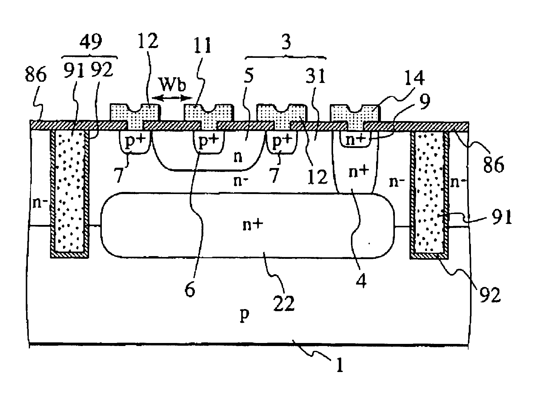
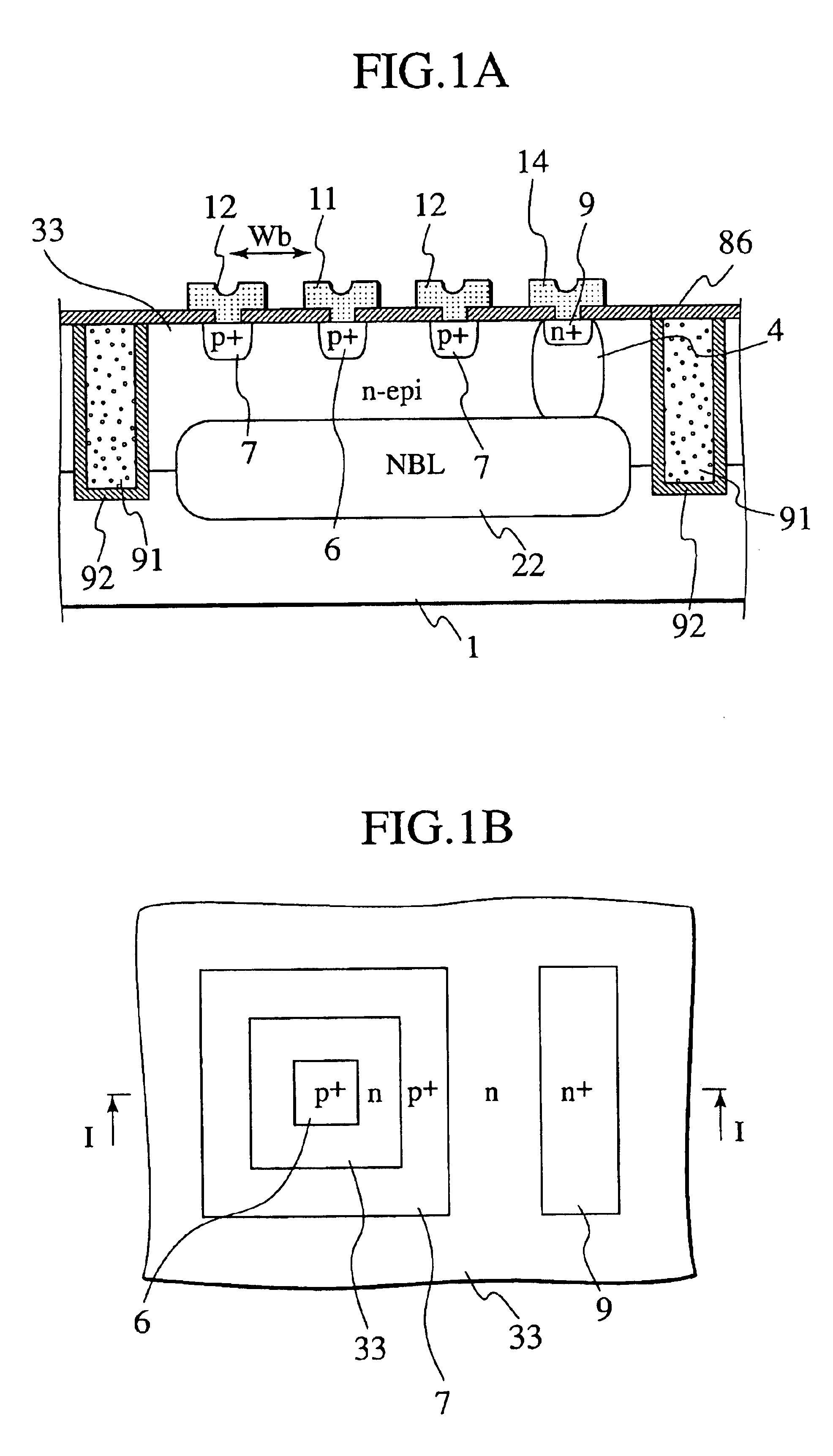
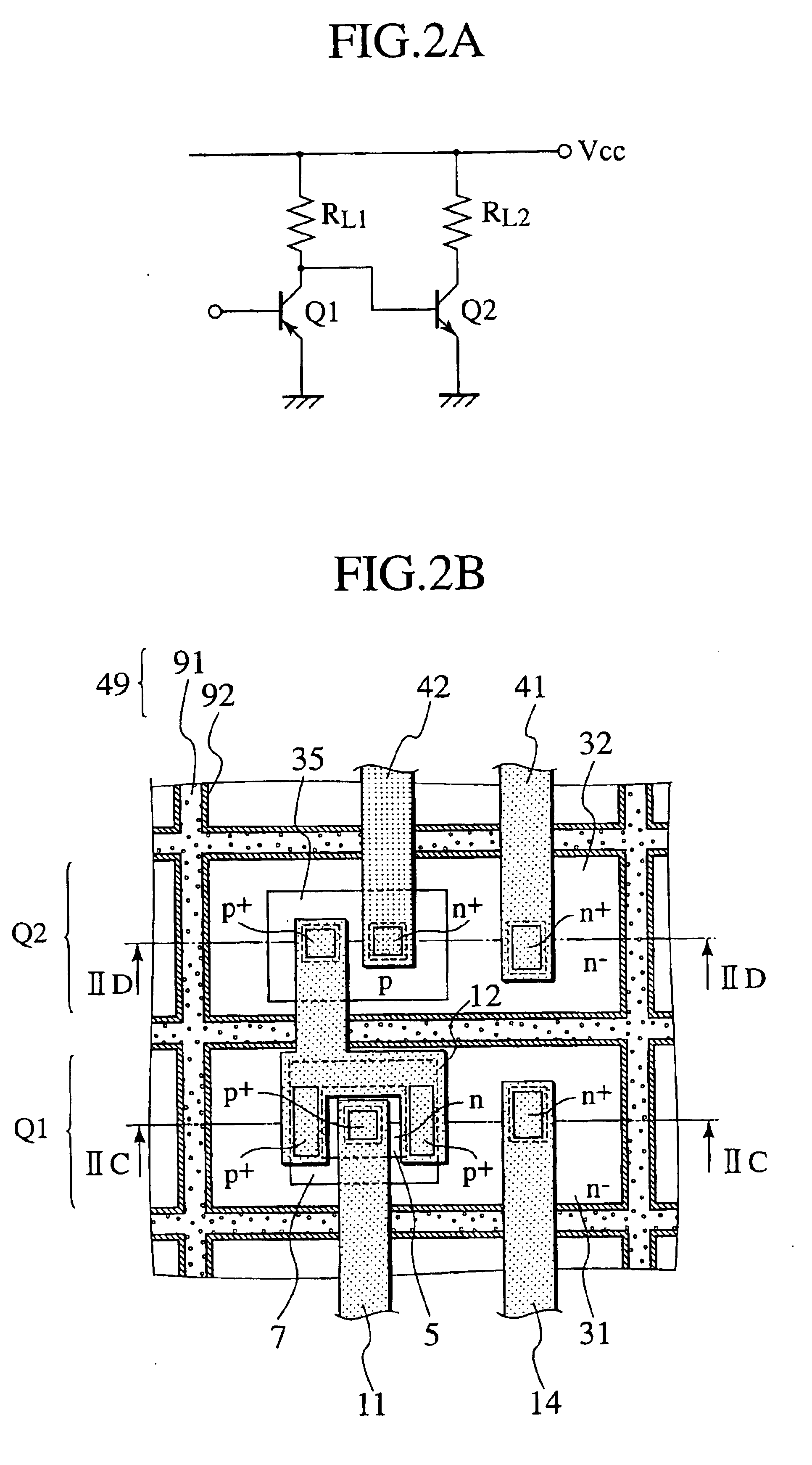
Various embodiments of the present invention will be described with reference to the accompanying drawings. It is to be noted that the same or similar reference numerals are applied to the same or similar parts and elements throughout the drawings, and the description of the same or similar parts and elements will be omitted or simplified. Generally and as it is conventional in the representation of semiconductor integrated circuits, it will be appreciated that the various drawings are not drawn to scale from one figure to another nor inside a given figure, and in particular that the layer thicknesses are arbitrarily drawn for facilitating the reading of the drawings. In the following description specific details are set fourth, such as specific materials, process and equipment in order to provide thorough understanding of the present invention. It will be apparent, however, to one skilled in the art that the present invention may be practiced without these specific details. In othe...


PUM


Abstract

The lateral pnp transistor encompasses a p-type semiconductor substrate, an n-type first buried region disposed on the semiconductor substrate, an n-type uniform base region disposed on the first buried region, an n-type first plug region disposed in the uniform base region, a p-type first emitter region and a first collector region disposed in and at the top surface of the uniform base region, a graded base region disposed in the uniform base region and a first base contact region disposed in the first plug region. The graded base region encloses the bottom and the side of the first main electrode region. The doping profile in the graded base region intervening between the first emitter region and the first collector region is such that the impurity concentration is gradually decreases towards the second main electrode region from the first main electrode region.

Description

1. Field of the InventionThe present invention relates to a semiconductor integrated circuit, more particularly to a structure of a lateral transistor suitable for implementing a high-density monolithic integration on a semiconductor substrate.2. Description of the Related ArtA structure merging a power transistor and its control circuit on the same semiconductor chip so as to form a semiconductor integrated circuit is known. In such a power IC, sometimes the power transistor is made by a vertical npn transistor and the control circuit by lateral pnp transistors, the lateral pnp transistor operating with relatively lower power than the vertical npn transistor. An example of the structure of the earlier lateral pnp transistor employed in these semiconductor integrated circuits (power ICs) is shown in FIGS. 1A and 1B. That is, the earlier lateral pnp transistor embraces a semiconductor substrate 1, an n-type first buried region 22 formed on the semiconductor substrate 1, an n-type fir...

Claims


Application Information

Patent Timeline
Patent Type & Authority Patents(United States)
IPC IPC(8): H01L29/02H01L29/10H01L29/735H01L29/66H01L29/36H01L21/8224H01L21/8228H01L27/082H01L21/331H01L29/732
CPCH01L29/1008H01L29/6625H01L29/735H01L29/36
Inventor YAMAMOTO, MAKOTOIWABUCHI, AKIO
Owner SANKEN ELECTRIC CO LTD
Why Eureka
Try Eureka