Apparatuses for heat-treatment of semiconductor films under low temperature

a technology of semiconductor films and apparatuses, applied in the field of apparatuses for heat treatment of semiconductor films under low temperature, can solve the problems of glass damage or distortion, high thermal budget, easy deformation of glass, etc., and achieve the effect of enhancing the motion of charged defects, high resistivity, and high resistivity

Inactive Publication Date: 2004-06-08
VIATRON TECH INC
View PDF3 Cites 19 Cited by
  • Summary
  • Abstract
  • Description
  • Claims
  • Application Information

AI Technical Summary

Benefits of technology

According to the apparatuses of the present invention, the semiconductor films can be heat-treated continuously and efficiently without damaging the thermally susceptible substrates: e.g., crystallization of amorphous silicon films at the minimum thermal budget acceptable for the use of glass, enhancing kinetics of dopant activation at the minimum thermal budget acceptable for the use of glass.
First mechanism is a selective joule heating of silicon films. Amorphous or polycrystalline silicon has high resistivity values at room temperature, for instance, 10.sup.6.about.10.sup.10 .OMEGA.-cm in the case of amorphous silicon. Thus, unless silicon is intentionally heated by external heat source, joule heating of silicon though said emf does not occur. However, when amorphous and polycrystalline Si are heated to elevated temperatures, their resistivities go down rapidly to the low values, for instance, 10.about.0.01 .OMEGA.-cm at 500.degree. C. Those resistivity values are similar to those of graphite (1.about.0.001 .OMEGA.-cm) and thus the induction-heating becomes possible. In spite of local heating of amorphous silicon under alternating magnetic flux, the glass substrate having high resistivity values (.about.10.sup.16 .OMEGA.-cm) is not heated by said alternating magnetic flux. Thus, the glass remains to be at low temperatures pre-set by the external heating.

Problems solved by technology

Glass is easily deformed when exposed to the temperature above 600.degree. C. for substantial length of time.
Those heat-treatments typically require high thermal budgets, unavoidably causing damage or distortion of glass.
However, high thermal budget of this method leads to damage and / or distortion of used glass substrates.
However, this method has critical drawbacks for its use in mass production.
The grain structure of poly-Si film through this process is extremely sensitive to the laser beam energy, so that the uniformity in grain structure and hence the device characteristics cannot be achieved.
Since it is difficult to precisely control the laser, the multiple shots introduce non-uniformities into the crystallization process.
Further, the surface of ELC poly-Si films is rough, which also degrades the performance of device.
The ELC also has the problem of hydrogen eruption when deposited amorphous Si has high hydrogen contents, which is usually the case in the plasma enhanced chemical vapor deposition (PECVD).
In addition to the problems in the area of processes, the system of ELC process equipment is complicated, expensive, and hard to be maintained.
This method, however, is limited by poor crystalline quality of poly-Si and metal contamination.
The metal contamination causes a detrimental leakage current in the operation of poly-Si TFTs.
Another problem of this method is a formation of metal silicides during the process.
The presence of metal silicides leads to an undesirable residue problem during the following etching process step.
This process requires high temperatures near 600.degree. C. and long duration time.
The problem which was found in the ELC for crystallization also exists here.
The rapid thermal changes during the ELC process leads to an introduction of high thermal stress to the poly-Si films as well as the glass, and hence, the deterioration of device reliability.
The problem of the RTA is that the photon radiation from those optical sources has the range of wavelength in which not only the silicon film but also the glass substrate is heated.
Therefore, the glass is heated and damaged during the process.

Method used


Image

  • Apparatuses for heat-treatment of semiconductor films under low temperature
  • Apparatuses for heat-treatment of semiconductor films under low temperature
  • Apparatuses for heat-treatment of semiconductor films under low temperature

Examples


Embodiment Construction

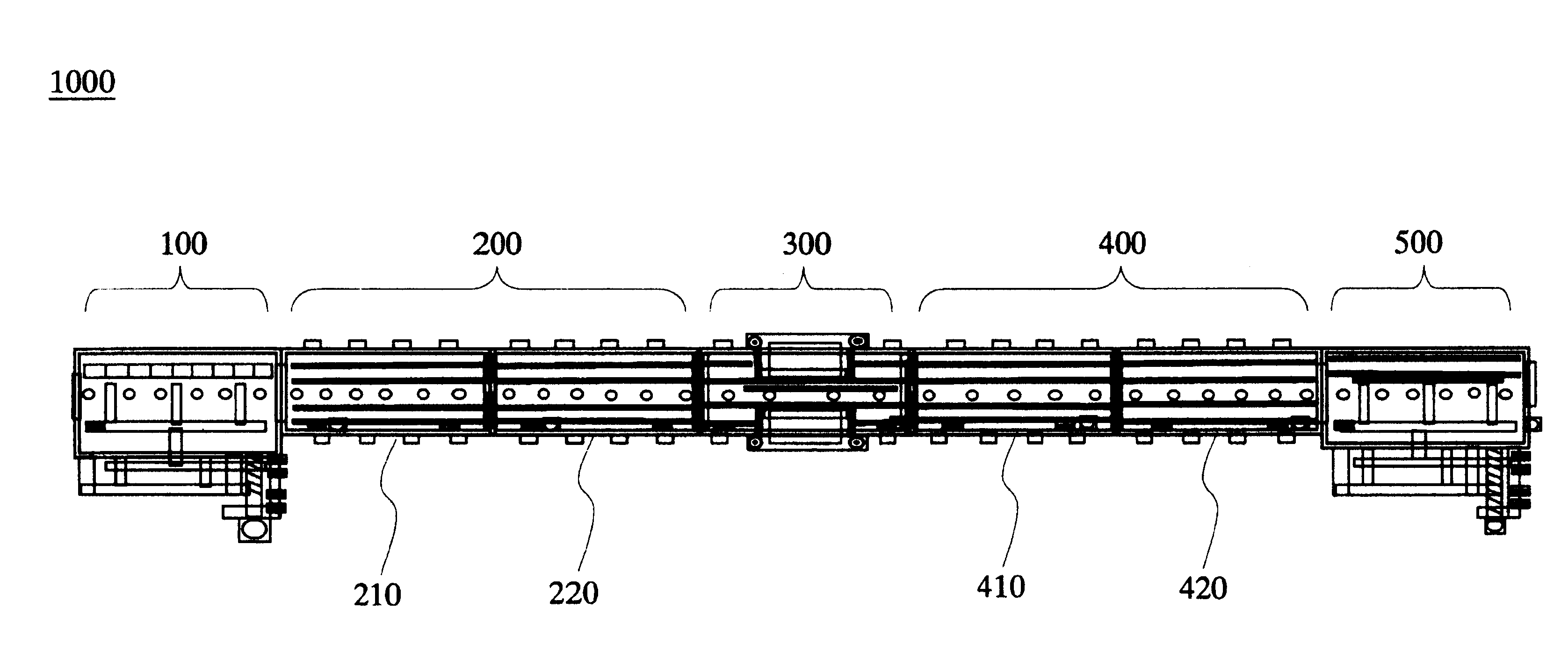
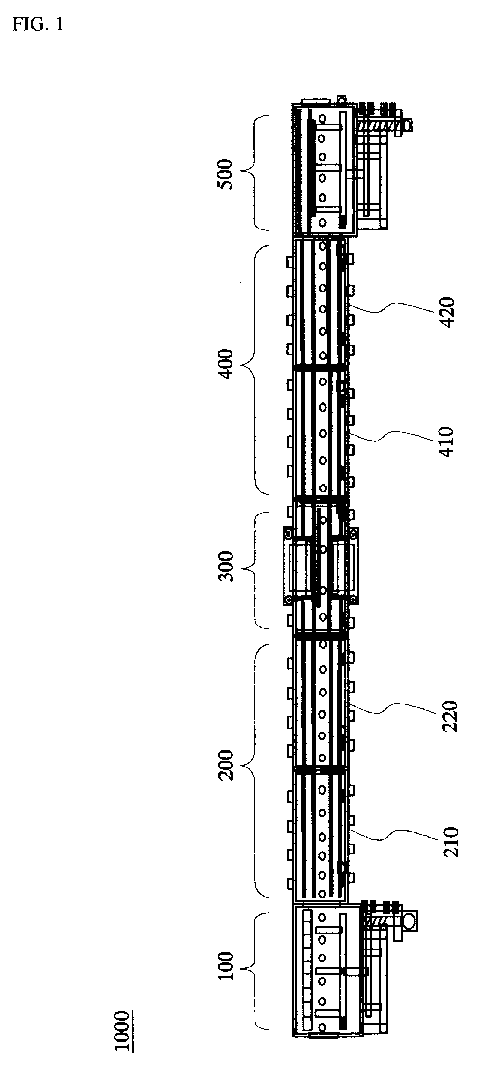
Referring to FIG. 1, a low-temperature heat-treatment system 1000 which includes a low-temperature heat-treatment apparatus according to the present invention consists of a supply member 100, a preheating member 200, an induction heating member 300, a cooling member 400, and a manufacture member 500, which are connected in serial for the continuous process. Each of the preheating member 200 and cooling member 400 has two chambers (210, 220, 410, 420) for consecutive heating and cooling of heat-treatment materials. The sudden change of temperature may lead damage of thermally susceptible non-conducting substrates, which is not desirable.

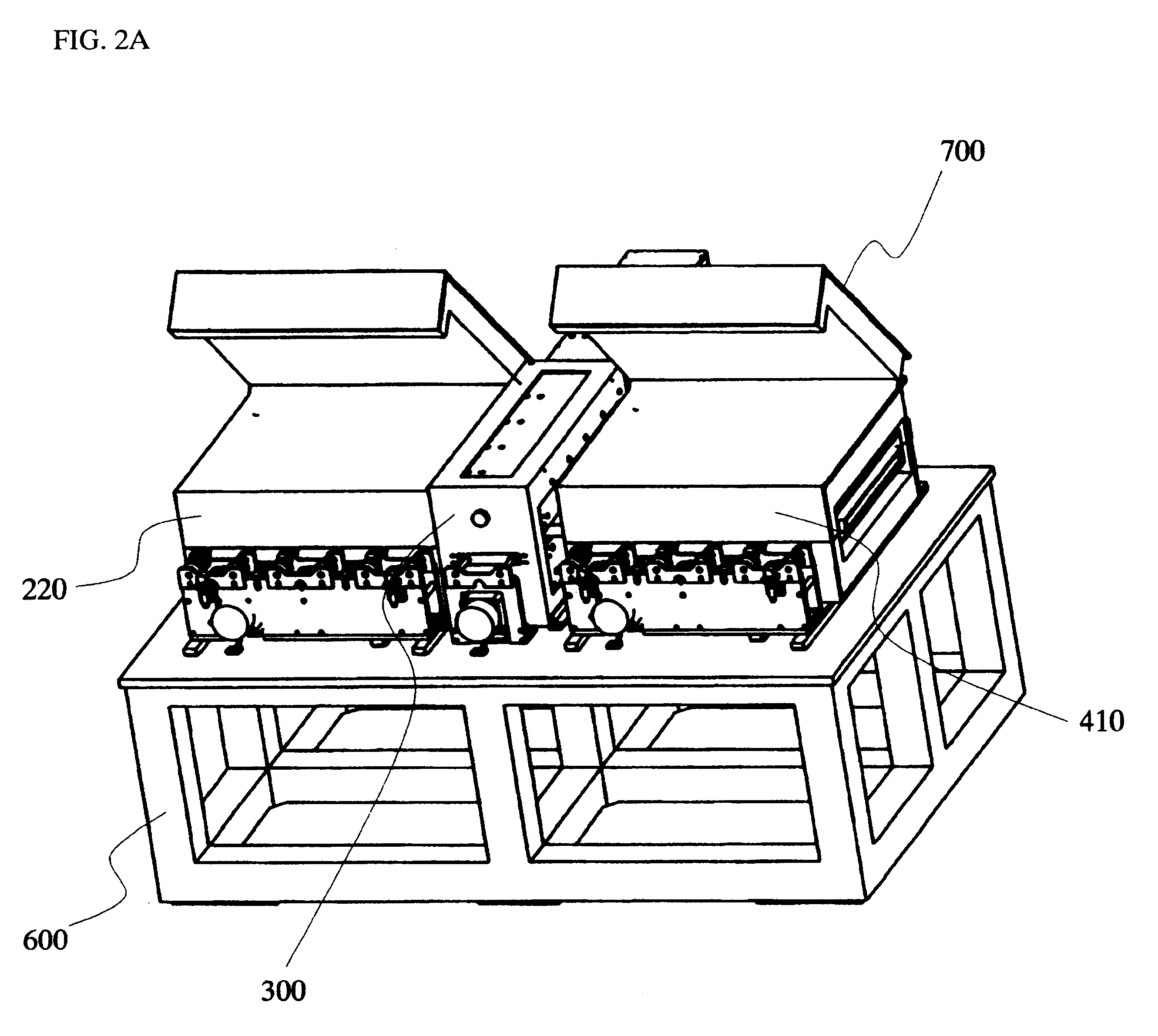
Referring to FIGS. 2A and 2B, a second preheating chamber 220, an induction-heating member 300 and a first cooling chamber 410 are mounted in serial on a table 600 for minimizing the external effect. Also, they have closing covers 700 for the facilitation of disorder check and exchange of components during the operation. In particular, the induction-h...


PUM

PropertyMeasurementUnit
temperatureaaaaaaaaaa
temperaturesaaaaaaaaaa
temperatureaaaaaaaaaa

Abstract

The present invention relates to apparatuses for continuous and efficient heat-treatment of semiconductor films upon thermally susceptible non-conducting substrates at a minimum thermal budget, and more particularly, to a polycrystalline silicon thin-film transistors (poly-Si TFTs) and PN diodes on glass substrates for various applications of liquid crystal displays (LCDs), organic light emitting diodes (OLEDs), and solar cells. According to the apparatuses of the present invention, the semiconductor films can be heat-treated without damaging the thermally susceptible substrates: e.g., crystallization of amorphous silicon films at the minimum thermal budget acceptable for the use of glass, enhancing kinetics of dopant activation at the minimum thermal budget acceptable for the use of glass.

Description

The present invention relates to apparatuses for continuous and efficient heat-treatment of semiconductor films upon thermally susceptible non-conducting substrates at a minimum thermal budget. More particularly, the invention relates to apparatuses for heat-treatment of preparing polycrystalline silicon thin-film transistors (poly-Si TFTs) and PN diodes on glass substrates for various applications of liquid crystal displays (LCDs), organic light emitting diodes (OLEDs), and solar cells.Liquid crystal displays (LCDs) and organic light emitting diodes (OLEDs) grow rapidly in the flat panel displays. In the present time, those display systems employ the active matrix circuit configuration using thin film transistors (TFTs). Fabrication of the TFTs on glass substrate is necessary in those applications.TFT-LCDs typically uses the TFTs composing amorphous Si films as an active layer (i.e., a-Si TFT LCD). Recently, interests on the development of TFTs using polycrystalline silicon films i...

Claims


Application Information

Patent Timeline
Patent Type & Authority Patents(United States)
IPC IPC(8): H01L21/00H05B6/02G02F1/1368H01L21/20H01L21/265H01L21/324H05B6/10H05B6/40
CPCH01L21/67109H05B6/105H01L21/324
Inventor KIM, HYOUNG JUNESHIN, DONG HOON
Owner VIATRON TECH INC
Why Eureka
Try Eureka