Cavity-structuralized silicon-carbon core-shell nanowire array, and preparation method and use thereof

A nanowire array and structured silicon technology, applied in nanotechnology, nanotechnology, structural parts, etc., can solve the problems of low area loading, short cycle life, and low material area specific capacity, achieving large capacity and low cost , the effect of improving electronic conductivity

Active Publication Date: 2016-03-30
THE NAT CENT FOR NANOSCI & TECH NCNST OF CHINA
View PDF6 Cites 19 Cited by
  • Summary
  • Abstract
  • Description
  • Claims
  • Application Information

AI Technical Summary

Problems solved by technology

[0005] The purpose of the present invention is to overcome the defects of low area loading, low area specific capacity and short cycle life of silicon negative electrode materials in the prior art, and provide a cavity structured silicon-carbon core-shell nanowire array and its preparation method , and the application of the silicon-carbon core-shell nanowire array as an anode material

Method used


Image

  • Cavity-structuralized silicon-carbon core-shell nanowire array, and preparation method and use thereof
  • Cavity-structuralized silicon-carbon core-shell nanowire array, and preparation method and use thereof
  • Cavity-structuralized silicon-carbon core-shell nanowire array, and preparation method and use thereof

Examples


Embodiment 1

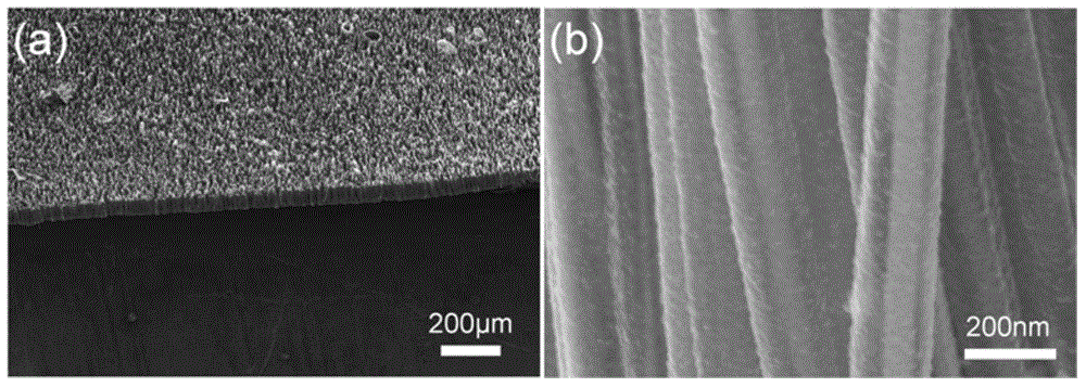
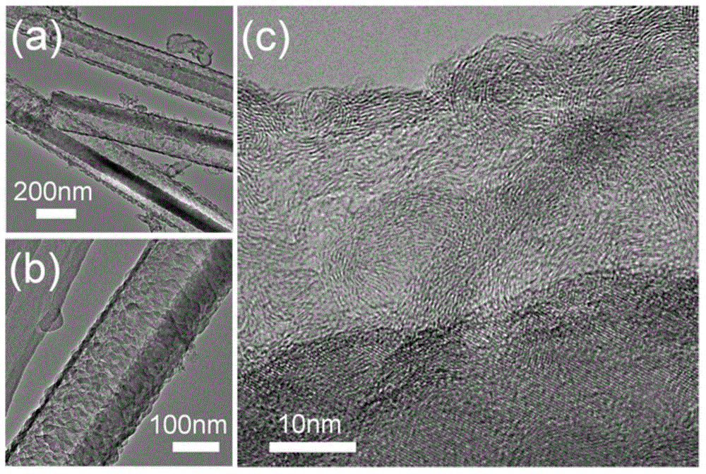
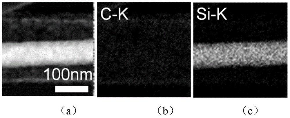
[0051] Take a single crystal silicon wafer, use evenly arranged polystyrene balls as a mask, deposit a gold film, put it in a plastic cup, add hydrogen peroxide and hydrofluoric acid aqueous solution, and keep it warm at 20°C for 60 minutes. A layer of silicon nanowire arrays is formed on the surface. After taking out the silicon wafer, rinse it with water, and then use aqua regia to remove the metal gold and then dry it. Then put it into a tube furnace, heat up to 700°C, keep it warm for 30 minutes, and then cool to room temperature. Inject argon-hydrogen mixed gas (2 / 1, v / v) with a total flow rate of 300 sccm. After the temperature is programmed to 1050° C., inject methane gas with a flow rate of 100 sccm. Turn off the methane gas after 5 minutes of constant temperature. After rapid cooling, take out the silicon wafer from the furnace, use hydrofluoric acid to remove silicon dioxide, and then immerse it in 5% sodium hydroxide aqueous solution at 90 ° C. After 60 minutes of r...

Embodiment 2

[0053] Take a single crystal silicon wafer, use uniformly arranged silicon oxide balls as a mask, deposit a gold film, put it in a plastic cup, add aqueous solution of hydrogen peroxide and hydrofluoric acid, keep it warm at 60°C for 30 minutes, the surface of the silicon wafer A layer of silicon nanowire array is formed, the silicon wafer is taken out, rinsed with water, and then dried with aqua regia to remove metal gold. Then put it into a tube furnace, raise the temperature to 500°C, keep it warm for 120 minutes and then cool it down. Inject argon-hydrogen gas mixture (1 / 1, v / v) with a total flow rate of 300 sccm. After the temperature is programmed to rise to 1050° C., methane begins to be introduced at a flow rate of 400 sccm. After constant temperature for 5 seconds, it is rapidly cooled. After cooling down to room temperature, take out the silicon wafer from the furnace, use hydrofluoric acid to remove silicon dioxide, and then immerse it in 5% sodium hydroxide aqueous...

Embodiment 3

[0055] Take a single crystal silicon wafer, use evenly arranged block copolymer (polystyrene-block-polyferrocenyldimethylsilane) balls as a mask, deposit a gold film, and put it in a plastic cup. Add an aqueous solution of hydrogen peroxide and hydrofluoric acid, keep warm at 45°C for 10 minutes, and a layer of silicon nanowire arrays is formed on the surface of the silicon wafer. After taking out the silicon wafer, rinse it with water, use aqua regia to remove the metal gold, and then dry it. Then put it into a tube furnace, raise the temperature to 300°C, keep it warm for 60 minutes and then cool it down. Hydrogen was introduced at a flow rate of 100 sccm. After the temperature was programmed to rise to 700° C., acetylene was introduced at a flow rate of 50 sccm. The temperature was kept constant for 5 minutes and then rapidly cooled. After cooling down to room temperature, take out the silicon wafer from the furnace, use hydrofluoric acid to remove the silicon dioxide, and ...


PUM

PropertyMeasurementUnit
lengthaaaaaaaaaa
thicknessaaaaaaaaaa
thicknessaaaaaaaaaa

Abstract

The invention relates to a cavity-structuralized silicon-carbon core-shell nanowire array, and a preparation method and a use thereof. The silicon-carbon core-shell nanowire array comprises a self-supporting structure and ordered silicon-carbon core-shell nanowires forming the structure, wherein an internal cavity exists between the core and the shell of each of the core-shell nanowires. The preparation method of the nanowire array comprises the following steps: chemically etching a silicon wafer, and forming a silicon nanowire array on the surface of the silicon wafer; heating the silicon nanowire array in air to form a silicon oxide layer on the surface of the silicon nanowire; depositing a carbon cladding layer on the silicon oxide coated silicon nanowire through a chemical vapor deposition technology, and removing the silicon oxide layer to prepare a silicon-carbon core-shell nanowire array with a cavity between the core and the shell; and peeling the cavity-structuralized silicon-carbon core-shell nanowire array from the silicon wafer through using an alkaline solution. The obtained self-supporting silicon-carbon core-shell nanowire array can be directly used as an active negative electrode, and has the characteristics of large capacity, stable circulation, long cycle life and practical application values.

Description

technical field [0001] The present invention relates to a cavity structured silicon-carbon core-shell nanowire array, a preparation method, its application as an anode material, and an electrochemical energy storage device using the silicon-carbon core-shell nanowire array as an anode material and / or energy storage systems. Background technique [0002] Lithium-ion batteries are ideal power sources for portable electronic devices and electric vehicles. The development of new electrodes with high energy density, long cycle life and high load capacity is currently a hot spot in the research field of lithium-ion batteries. Silicon is a new type of negative electrode material for lithium-ion batteries. Its lithium storage reaction voltage platform is low, and its theoretical capacity is extremely high (4200mAh / g), which is much higher than the current marketed graphite negative electrode. Silicon is abundant in nature. It is a kind of lithium-ion battery anode material with g...

Claims


Application Information

Patent Timeline
Patent Type & Authority Applications(China)
IPC IPC(8): H01M4/36H01M4/62H01M4/134B82Y30/00H01M10/0525
CPCY02E60/10
Inventor 李祥龙王斌智林杰
Owner THE NAT CENT FOR NANOSCI & TECH NCNST OF CHINA
Why Eureka
Try Eureka