

Adhesion type area sensor and display device having adhesion type area sensor
a display device and adhesion-type technology, which is applied in the field of adhesion-type area sensors and display devices having image sensor functions, can solve the problems of affecting the size of the backlight 2502 and the size of the light scattering plate 2503, reducing the size of the area sensor itself, and reducing the size of the backlight 2502
- Summary
- Abstract
- Description
- Claims
- Application Information
AI Technical Summary
Benefits of technology
Problems solved by technology
Method used
Image

Examples
embodiment 1
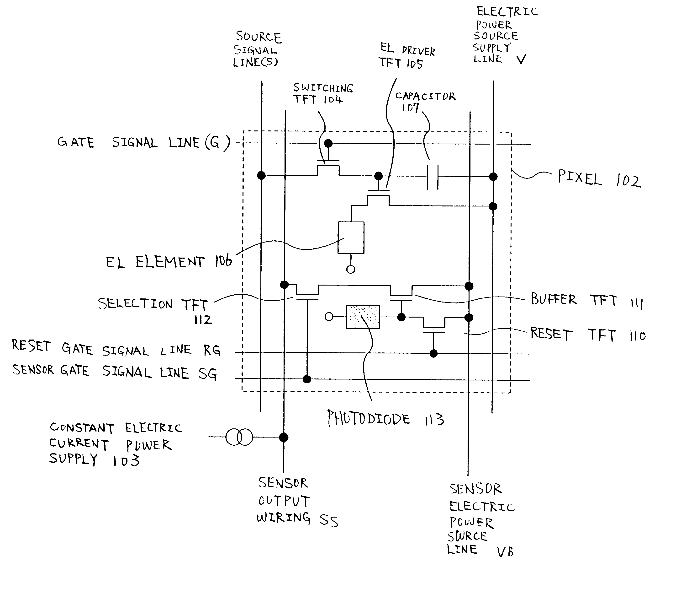
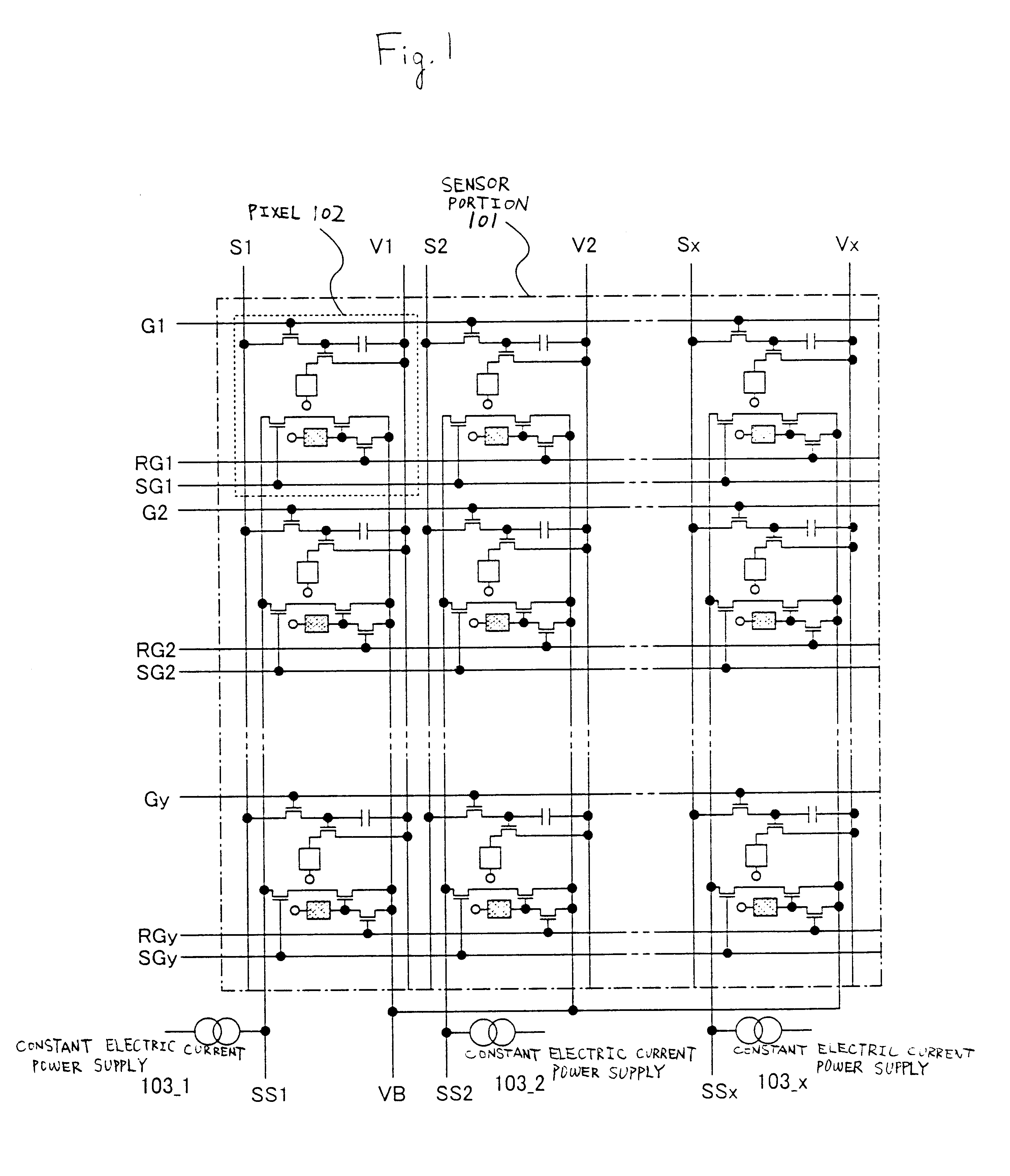
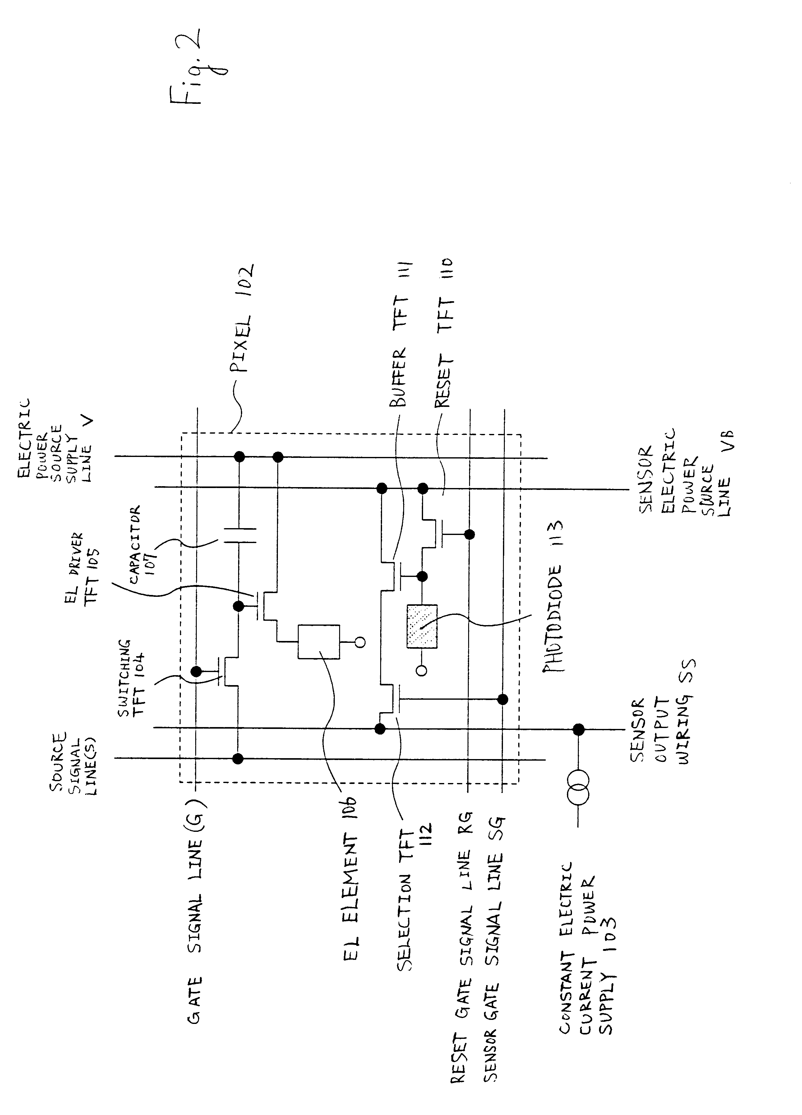
A method of driving the switching TFT 104 and the EL driver TFT 105, which control the operation of the EL element 106 shown in FIG. 2, is explained in Embodiment 1. Note that the structure of the sensor portion is the same as that of the embodiment mode, and therefore FIG. 1 and FIG. 2 are referenced.
FIG. 5 shows a top view of an area sensor of Embodiment 1. Reference numeral 120 denotes a source signal line driver circuit, reference numeral 122 denotes a gate signal line driver circuit, and both control the driving of the switching TFT 104 and the EL driver TFT 105. Further, reference numeral 121 denotes a sensor source signal line driver circuit, reference numeral 123 denotes a sensor gate signal line driver circuit, and both control the driving of the reset TFT 110, the buffer TFT 111, and the selection TFT 112. Note that the source signal line driver circuit 120, the gate signal line driver circuit 122, the sensor source signal line driver circuit 121, and the sensor gate signa...
embodiment 2
A method of driving the switching TFT 104 and the EL driver TFT 105 when displaying an image in the sensor portion 101 is explained in Embodiment 2. Note that the structure of the sensor portion is the same as the structure shown by the embodiment mode, and therefore FIG. 1 and FIG. 2 may be referenced.
A timing chart when performing display of an image in the sensor portion 101 in the area sensor of the present invention by a digital method is shown in FIG. 7.
First, one frame period F is divided into n subframe periods SF1 to SFn. The number of subframe periods in one frame period also increases as the number of gray scales increases. Note that, when the sensor portion of the area sensor displays an image, one frame period F denotes a period during which all pixels of the sensor portion display one image.
It is preferable that 60 or more frame periods be provided each second for the case of Embodiment 2. By setting the number of images displayed each second to 60 or greater, it becom...
embodiment 3
The electric potential of the opposing electrodes are maintained at the same electric potential as that of the electric power source potential during the address period in Embodiments 1 and 2. Therefore, the EL elements do not emit light. However, the present invention is not limited to this structure. If an electric potential difference is always formed between the opposing electric potential and the electric power source potential, on an order at which the EL elements will emit light, when the electric power source potential is applied to the pixel electrodes, display may also be performed in the address period, similar to the display period.
However, when combining Embodiment 1, in which the EL elements are used as the light source of the area sensor, with Embodiment 3, it is important that the sensor frame period SF be contained within the frame period for an area sensor which reads in a single color image. Furthermore, it is important that the three subframe periods correspondin...
PUM
 Abstract
Description
Claims
Application Information