Electronic circuit equipment using multilayer circuit board

a multi-layer circuit board and circuit technology, applied in the direction of printed circuit non-printed electric components association, electrical connection formation of printed elements, electrical apparatus construction details, etc., can solve the problems of ceramic, i, and light weight of the board

Inactive Publication Date: 2004-06-29
RENESAS ELECTRONICS CORP
View PDF10 Cites 93 Cited by
  • Summary
  • Abstract
  • Description
  • Claims
  • Application Information

AI Technical Summary

Benefits of technology

The employment of the method like this makes it possible to use, as the first electrode, a metal on the top portion of which the thin film dielectric can be grown epitaxially. The employment thereof also allows a high electrical-conductivity metal to be used as the first wiring conductor. As a result, it becomes possible to form, inside the multilayer circuit board, the thin film capacitor including the high dielectric-constant thin film dielectric.
Also, of the first electrode and the second electrode, an electrode that is positioned nearer to a transmission-line conductor formed on the multilayer circuit board is set at the grounding potential. This setting makes it possible to reduce a signal interference between the transmission line and the electrode that has not been set at the grounding potential within the thin film capacitor having a capacity value with respect to the grounding potential. Consequently, no deterioration occurs in the performance of the electronic circuit equipment.

Problems solved by technology

Attention, however, is now focused on a resin-based board with passive elements built in, because such a board is light-weight, not subject to cracking, inexpensive, etc.
In the conventional multilayer circuit package that U.S. Pat. No. 5,027,253 has proposed, there existed a problem that it is difficult to cause a ceramic, i.e., the dielectric material, to grow epitaxially on the first signal core.
Moreover, when employing the easily oxidized metal such as copper or aluminum as the first signal core, sputtering the oxide ceramic thereon resulted in the following problem or the like: The sputtering oxidizes the surface of the metal that forms the first signal core, thereby forming an oxide layer other than the ceramic thin film.
This increases the thickness of the dielectric layer, thus lowering the capacity value.
If the capacitor and the signal line intersect to each other, a signal interference occurs therebetween, thereby resulting in a problem that a deterioration occurs in the performance of the electronic circuit using this multilayer circuit board.
However, if precision capacitors, e.g., impedance-matching capacitors, are built inside the multilayer circuit board, manufacturing variations in the capacity values become a serious problem.

Method used


Image

  • Electronic circuit equipment using multilayer circuit board
  • Electronic circuit equipment using multilayer circuit board
  • Electronic circuit equipment using multilayer circuit board

Examples


first embodiment

1. First Embodiment

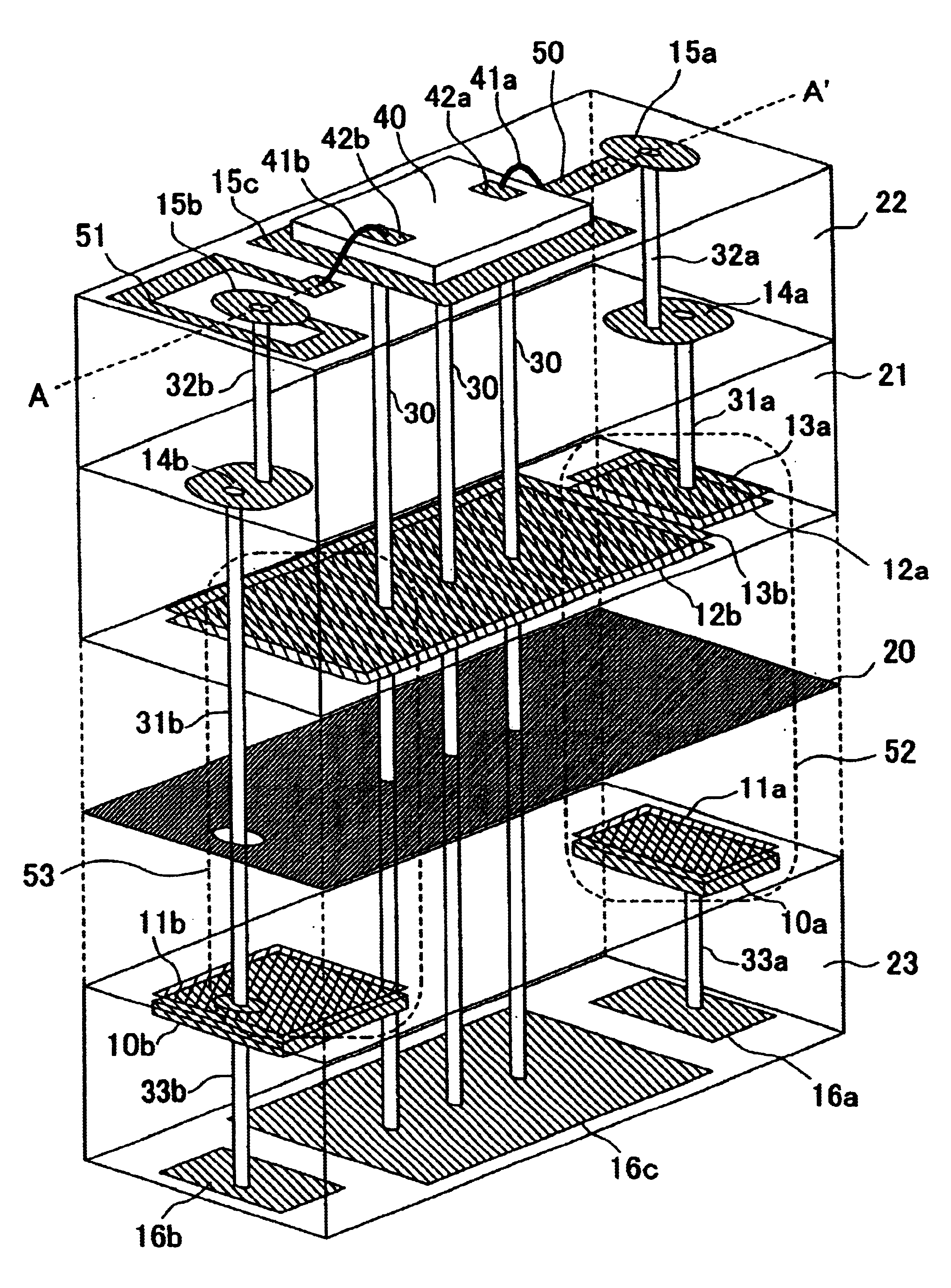
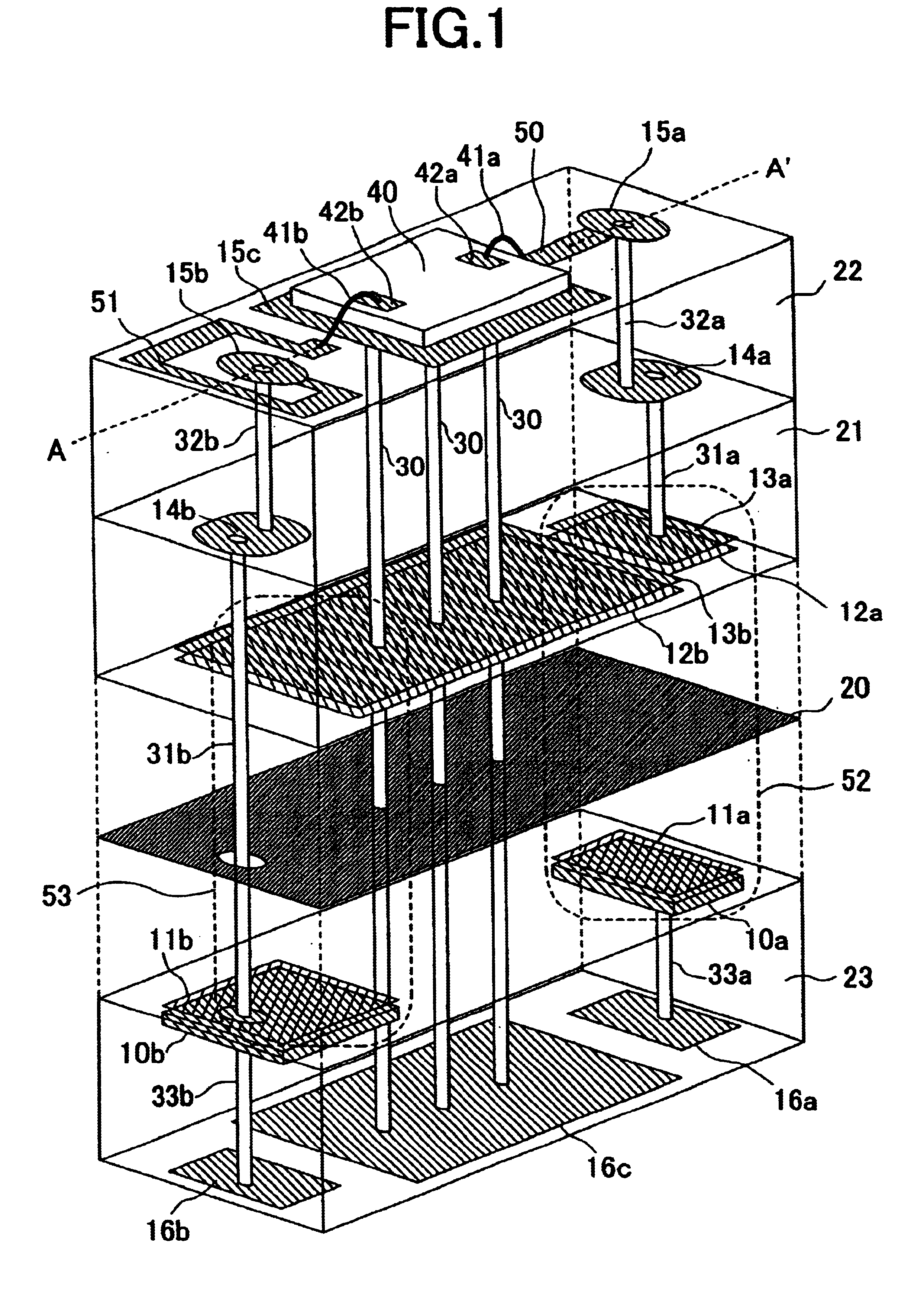
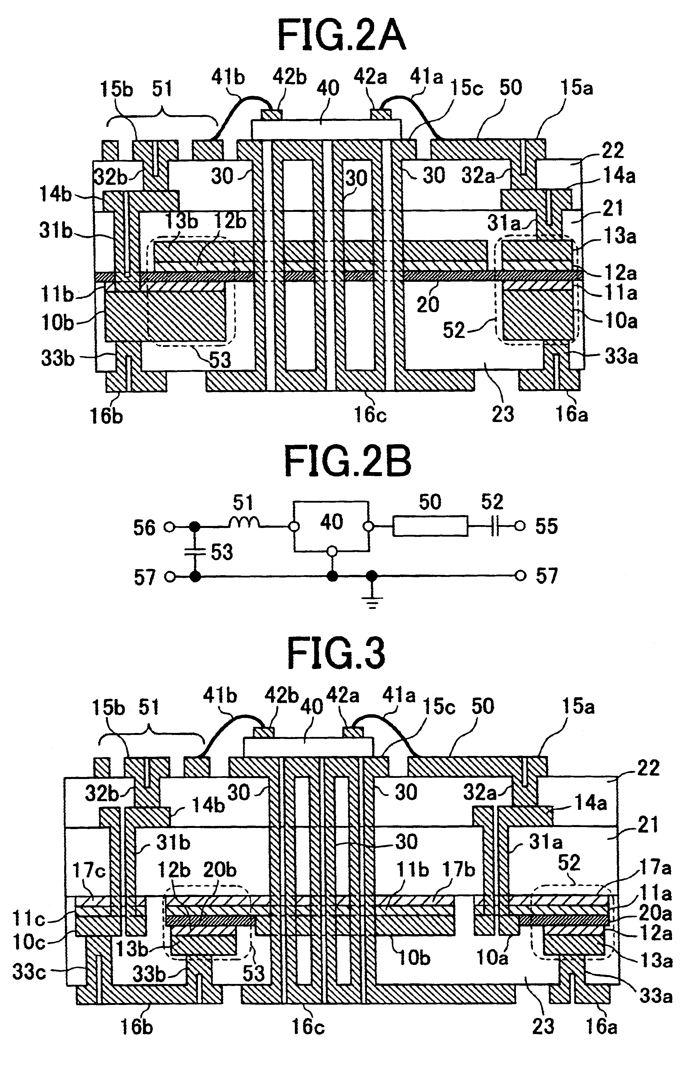
Using FIG. 1 and FIGS. 2A and 2B, the explanation will be given below concerning the first embodiment of the present invention. FIG. 1 is a perspective view of the electronic circuit equipment using the multilayer circuit board in the first embodiment. FIG. 2A is a cross-sectional view of the electronic circuit equipment cut off along a one-point chain line A--A' in FIG. 1. FIG. 2B is a diagram of the equivalent circuit for the electronic circuit equipment.

A thin film dielectric 20 is sandwiched between a first electrode 11a and a second electrode 13a that overlays the first electrode to each other, thereby forming a thin film capacitor 52. A second connection layer 12a the area of which is equal to that of the second electrode 13a is provided between the second electrode 13a and the thin film dielectric 20. A first wiring conductor 10a the area of which is equal to that of the first electrode 11a is provided on a plane of the first electrode 11a opposite to the t...

second embodiment

2. Second Embodiment

FIG. 3 is a cross-sectional view of the electronic circuit equipment using the multilayer circuit board for explaining a second embodiment of the present invention. The equivalent circuit for the present electronic circuit equipment is the same as the one used in the first embodiment and illustrated in FIG. 2B.

A thin film dielectric 20a is sandwiched between the first electrode 11a and the second electrode 13a, thereby forming the thin film capacitor 52. The second connection layer 12a is provided between the second electrode 13a and the thin film dielectric 20a. The second electrode 13a is connected to the back-surface conductor 16a via the via-hole 33a provided in the dielectric layer 23. A first connection layer 17a is provided on a plane of the first electrode 11a opposite to the thin film dielectric 20a. The first wiring conductor 10a is provided at a portion of the first electrode 11a which is positioned on the thin film dielectric 20a side and does not ove...


PUM


Abstract

In an electronic circuit equipment using a multilayer circuit board on which a semiconductor chip is mounted, a thin film capacitor is provided on the multilayer circuit board. Moreover, a first electrode of the thin film capacitor and a first wiring of the multilayer circuit board are electrically connected to each other, and a second electrode of the thin film capacitor and a second wiring of the multilayer circuit board are electrically connected to each other, respectively. Furthermore, a thin film dielectric of the thin film capacitor was grown epitaxially with the first electrode as its base. The employment of the multilayer circuit board makes it possible to provide the electronic circuit equipment using the multilayer circuit board that includes the built-in thin film capacitor having the high dielectric-constant thin film dielectric.

Description

1. Field of the InventionThe present invention relates to electronic circuitry using a multilayer circuit board that includes a buried capacitor.2. Description of the Prior ArtIn accompaniment with the downsizing of portable equipment, a technology for forming a passive component such as a capacitor within the board in order to enhance the mounting density has become more prevalent, especially in cellular phones. The technology that is in the mainstream at present employs a ceramic board. Attention, however, is now focused on a resin-based board with passive elements built in, because such a board is light-weight, not subject to cracking, inexpensive, etc. When forming a capacitor within a board, employing a thin film capacitor whose capacitive density can be made higher is advantageous in downsizing the board. U.S. Pat. No. 5,027,253 has disclosed a conventional technology concerning a board in which the thin film capacitor is buried. This technology will be explained below, using ...

Claims


Application Information

Patent Timeline
Patent Type & Authority Patents(United States)
IPC IPC(8): H01L21/02H01L23/498H01L21/48H01L23/48H05K1/16H05K3/42H05K3/46H05K1/02H01L23/12H01L25/00
CPCH01L21/4857H01L23/49822H05K1/162H01L23/49883H01L23/49894H01L2224/48091H01L2224/48227H01L2224/48465H01L2924/01004H01L2924/0102H01L2924/01039H01L2924/01046H01L2924/01078H01L2924/01079H01L2924/19041H01L2924/3011H05K1/0206H05K3/429H05K3/4644H05K2201/0175H05K2201/0179H05K2201/09509H05K2201/09536H01L2924/00014H01L24/48H01L2924/00H01L2224/45147H01L2924/01047H01L24/45H01L2224/05553H01L2924/10161
Inventor OKABE, HIROSHIYAMADA, HIROZI
Owner RENESAS ELECTRONICS CORP
Why Eureka
Try Eureka