Display device

a display device and display screen technology, applied in the direction of static indicating devices, instruments, transistors, etc., can solve the problems of distortion at the interface, difficult to reduce the size of the display device, and difficult to make the required area of the tab small

Inactive Publication Date: 2004-07-06
SEMICON ENERGY LAB CO LTD
View PDF13 Cites 73 Cited by
  • Summary
  • Abstract
  • Description
  • Claims
  • Application Information

AI Technical Summary

Problems solved by technology

With the passive type EL display device, in the case of employing the TAB for assembling the signal line driving circuit, there is the problem that an area required for the TAB is difficult to be made small, so reduction in the size of the display device is difficult.
This poses the problem that a distortion is induced at the interface by a temperature change on account of the difference between the thermal expansion coefficients of the substances.
The distortion disturbs the structure of the driving circuit, and forms one of causes for spoiling the reliability of the passive type EL display device.
This poses the problem that, as the pixel becomes smaller, a proportion occupied by the transistors within the pixel enlarges more, so the aperture factor of the pixel, in turn, the display device lessens.
Heretofore, in the passive type EL display device, it has been one of causes for spoiling the reliability of the display device that the signal line driving circuit formed on a semiconductor substrate is bonded onto the pixel portion substrate.

Method used


Image

  • Display device
  • Display device
  • Display device

Examples


embodiment 1

[Embodiment 1]

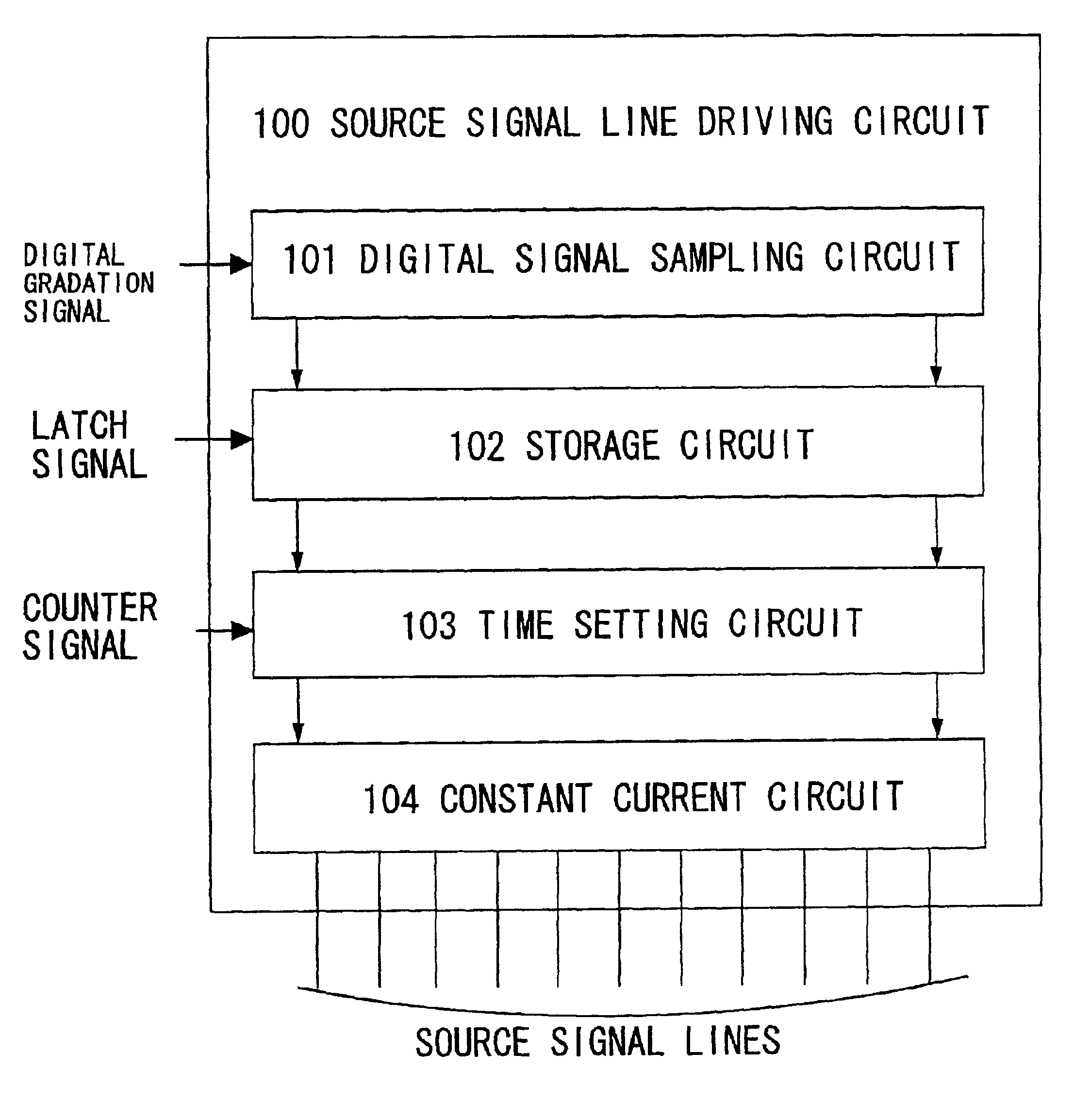
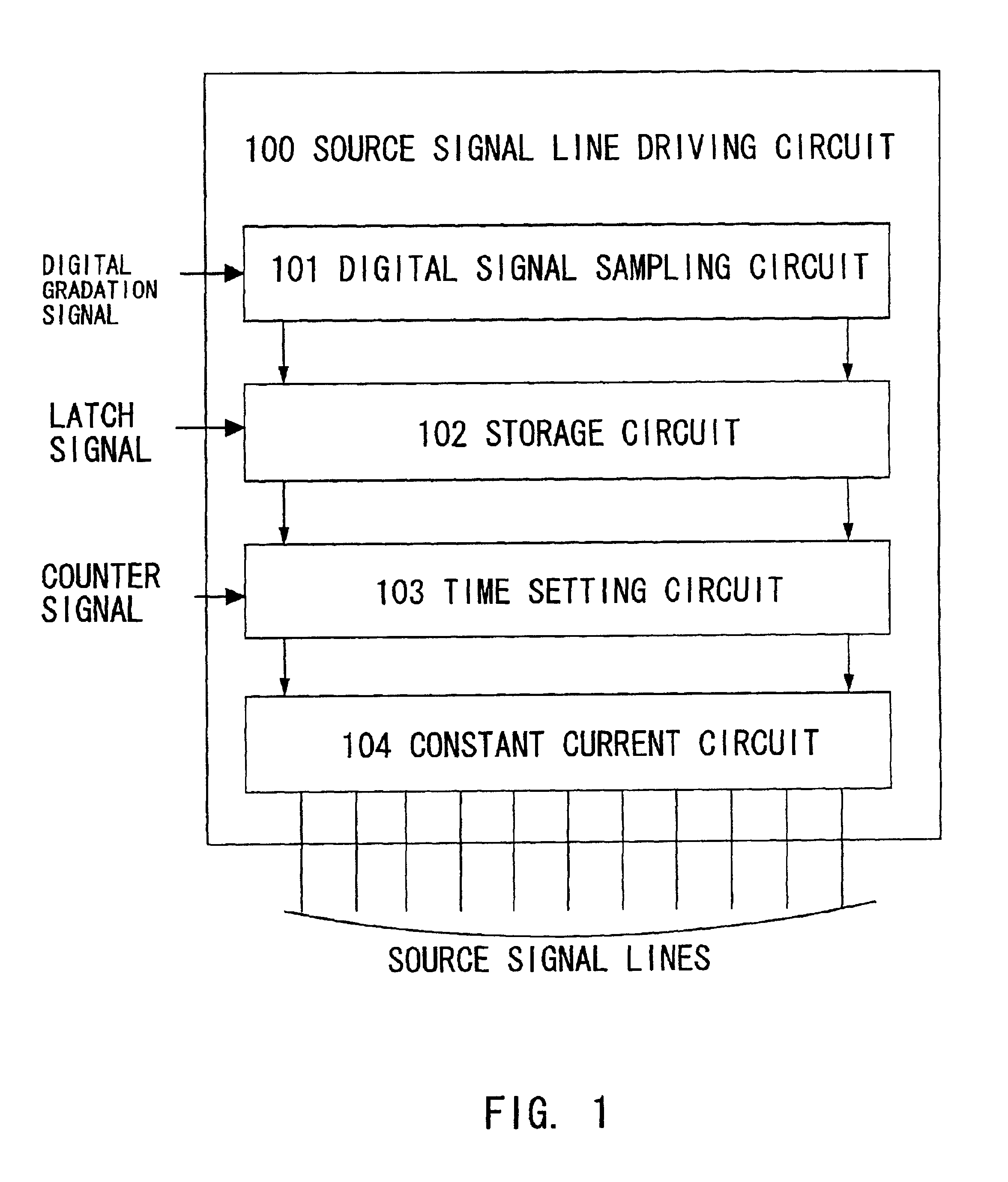
FIG. 7 shows the construction and driving method of the source signal line driving circuit of an EL display device embodying the present invention.

This embodiment will be described the source signal line driving circuit which outputs signals to x source signal lines.

A digital signal sampling circuit 201 and a storage circuit 202 are constructed of a shift register 203, a latch circuit 1 (204a) and a latch circuit 2 (204b).

A digital gradation signal VD is inputted to the digital signal sampling circuit 201. Here in this embodiment, the source signal line driving circuit corresponding to the digital gradation signal of 4 bits is mentioned as an example. However, the present invention is not restricted to the example, but it is also applicable to a digital gradation signal of 6 bits, 8 bits or any other bits.

The signals of the digital gradation signal VD sampled by the digital signal sampling circuit 201 are sequentially inputted to the latch circuit 1 (latches LAT1,1-LAT...

embodiment 2

[Embodiment 2]

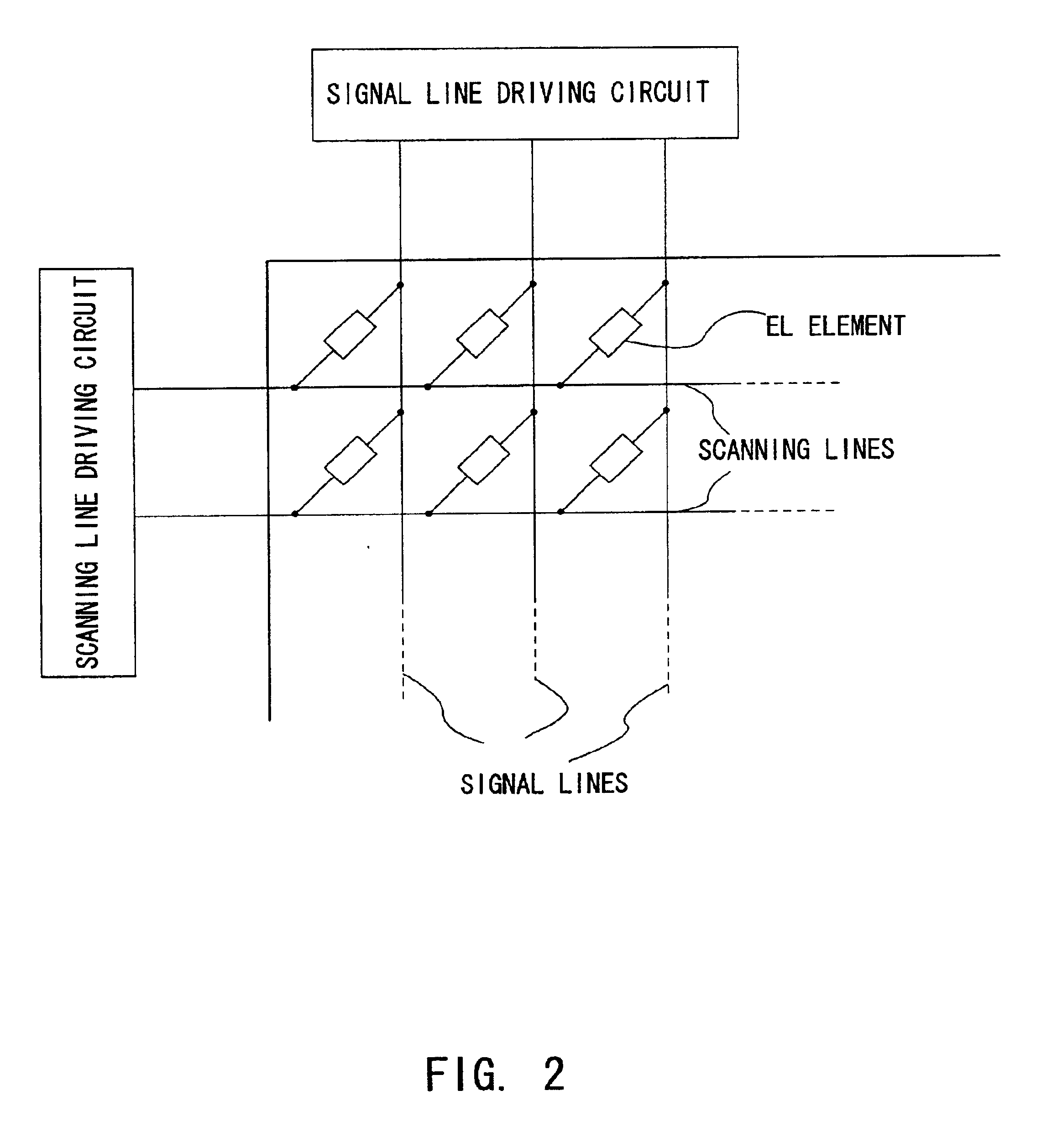
FIG. 13 shows the construction of the pixel portion of an active type EL display device embodying the present invention.

Gate signal lines (G1-Gy) to which selection signals from a gate signal line driving circuit are respectively inputted, are connected to the gate electrodes of switching TFTs included in individual pixels. Besides, either regions of the source regions and drain regions of the switching TFTs included in the individual pixels are connected to source signal lines (S1-Sx) to which currents are respectively inputted, while the other regions are connected to EL elements included in the individual pixels.

By the way, in the present invention, each of the switching TFTs may be either an n-channel TFT or a p-channel TFT.

The driving method of the active type EL display device in this embodiment will be described. When the gate signal line G1 is selected, all the switching TFTs connected thereto have a voltage applied to their gate electrodes and fall into ON sta...

embodiment 3

[Embodiment 3]

In this embodiment, there will be described a case where the source signal line driving circuit of Embodiment 1 is employed for the active type EL display device of Embodiment 2.

That is, there will be described a case where the source signal line driving circuit as explained in Embodiment 1, which outputs the constant currents to the source signal lines for the time periods corresponding to the inputted sampled digital gradation signals, is applied to the active type EL display device as explained in Embodiment 2, in which each pixel is constructed of one TFT and one EL element.

The current to be inputted to each of the source signal lines of the active type EL display device of Embodiment 2 is generated by the source signal line driving circuit explained in Embodiment 1.

As explained before, the current which is outputted from the source signal line driving circuit according to the present invention is the current pulse having the duration which corresponds to the sampl...


PUM


Abstract

A signal line driving circuit which includes a digital signal sampling circuit, a storage circuit, a time setting circuit and a constant current circuit, is fabricated of TFTs on an insulating substrate which is made of the same substance as that of a pixel portion substrate. Thus, in a passive type EL display device, the problem of a distortion in the case of bonding the signal line driving circuit onto the pixel portion substrate can be eliminated. Besides, in an active type EL display device, each pixel is constructed of one transistor and an EL element. Thus, the aperture factor of the EL display device is enlarged.

Description

1. Field of the InventionThe present invention relates to an electronic display device which is formed having an EL (electroluminescent) element on a substrate. More particularly, it relates to a display device which employs a semiconductor element (an element including a semiconductor thin film). Also, it relates to an electronic equipment whose display portion includes an EL display device.2. Description of the Related ArtIn recent years, EL display devices each having an EL element as a self-emission type element have been vigorously developed. The EL display device is also called the "organic EL display (OELD)" or "organic light emitting diode (OLED)".Unlike a liquid crystal display device, the EL display device is of self-emission type. The EL element has a construction wherein an EL layer is sandwiched in between a pair of electrodes (an anode and a cathode), and wherein the EL layer has a multilayer structure ordinarily. Typically mentioned is the multilayer structure of "hol...

Claims


Application Information

Patent Timeline
Patent Type & Authority Patents(United States)
IPC IPC(8): G09G3/30H01L21/02H01L21/336H01L21/70H01L27/12H01L29/66H01L21/84H01L29/786G09G3/20H01L21/77
CPCG09G3/30H01L29/66757H01L29/78621H01L29/78645G09G3/2014G09G2300/08G09G2310/027H01L27/12H01L27/1214H01L2029/7863H01L27/1259H01L27/127
Inventor KOYAMA, JUN
Owner SEMICON ENERGY LAB CO LTD
Why Eureka
Try Eureka