Method for stacking semiconductor die within an implanted medical device

a medical device and semiconductor technology, applied in semiconductor devices, semiconductor/solid-state device details, electrical apparatus, etc., can solve the problems of limiting the monitoring of the heart, the inability of electronic monitors to be useful in controlling the activity of the human body, and the complexity of the problem

Inactive Publication Date: 2004-08-24
MEDTRONIC INC
View PDF15 Cites 42 Cited by
  • Summary
  • Abstract
  • Description
  • Claims
  • Application Information

AI Technical Summary

Problems solved by technology

These types of electronic devices have proven to be accurate and reliable in operation, but initially were generally limited to monitoring the heart, as opposed to controlling or assisting the heart, owing principally to their size and power requirements.
Outside the laboratory or hospital these electronic monitors did not prove useful in controlling the activity of the human body, such as the heart.
As pacemakers have become more sophisticated, monitoring more functions and implementing more sophisticated control techniques, their complexity has increased dramatically.
Increased functionality and complexity have lead to more complex, and thus, larger circuitry.
Implantability of these devices, however, suffers with increased size.

Method used


Image

  • Method for stacking semiconductor die within an implanted medical device
  • Method for stacking semiconductor die within an implanted medical device
  • Method for stacking semiconductor die within an implanted medical device

Examples


Embodiment Construction

Illustrative embodiments of the invention are described below. In the interest of clarity, not all features of an actual implementation are described in this specification. It will of course be appreciated that in the development of any such actual embodiment, numerous implementation-specific decisions must be made to achieve the developers' specific goals, such as compliance with system-related and business-related constraints, which will vary from one implementation to another. Moreover, it will be appreciated that such a development effort might be complex and time-consuming, but would nevertheless be a routine undertaking for those of ordinary skill in the art having the benefit of this disclosure.

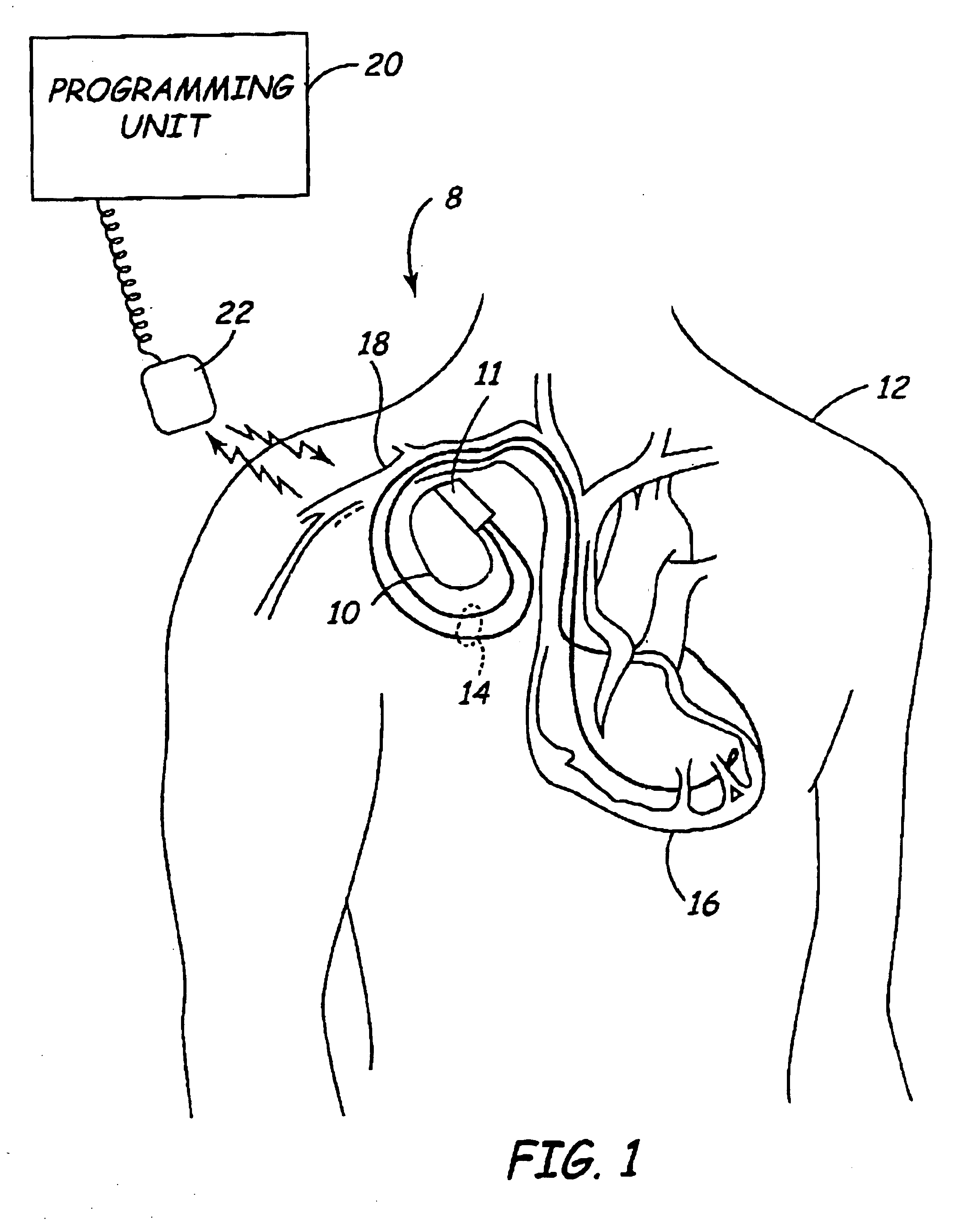
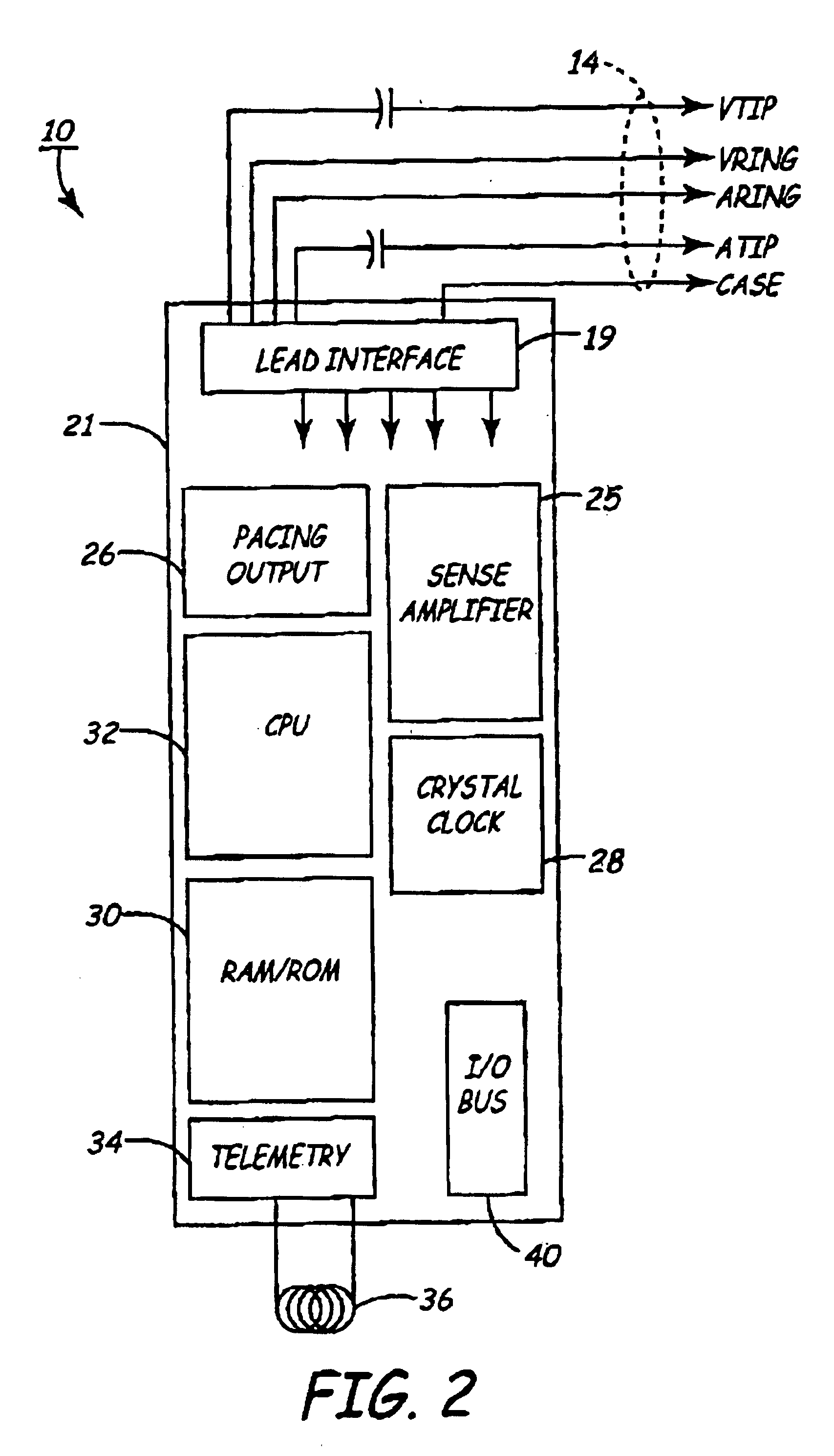
FIG. 1 illustrates an implantable medical device (IMD) system 8, which includes, for example, an implantable pacemaker 10 that has been implanted in a patient 12. The pacemaker 10 is housed within a hermetically sealed, biologically inert outer canister or housing, which may be conduct...


PUM


Abstract

A method for forming a stackable wafer for use in an implantable device is provided. The method comprises forming an opening extending substantially through the wafer. Thereafter, conductive material is deposited within the opening to substantially fill the opening. A bump is then formed on an upper surface of the wafer adjacent the conductive material, and a contact pad is formed on a lower surface of the wafer adjacent the conductive material. A second wafer formed using substantially the same process may then be stacked on top of the first wafer with the bump of the first wafer being in contact with the contact pad of the second wafer. A soldering process may then be used to couple the adjacent pad and wafer for physically mounting the wafers and providing electrical connectivity therebetween.

Description

1. Field of the InventionThis invention relates generally to a method for packaging semiconductor devices in an implantable device, and, more particularly, to a method and apparatus for providing electrical connectivity between a plurality of stacked semiconductor devices in an implantable device.2. Description of the Related ArtElectronic devices that monitor or otherwise interact with human bodies have been in widespread use for some time now. For example, electronic devices and sensors have been routinely used to measure muscular activity. That is, electronic devices are commonly used to detect and graph electrical activity representative of a beating human heart. Electrocardiograms (EKGs), which are produced by such electronic devices, are routinely used by doctors and / or technicians as diagnostic aids to evaluate the condition of a patient's heart.These types of electronic devices have proven to be accurate and reliable in operation, but initially were generally limited to moni...

Claims


Application Information

Patent Timeline
Patent Type & Authority Patents(United States)
IPC IPC(8): H01L21/60H01L21/02H01L25/065H01L23/48H01L21/70H01L21/768
CPCH01L21/76898H01L23/481H01L24/11H01L25/0657H01L25/50H01L2224/13099H01L2225/06513H01L2225/06541H01L2924/01013H01L2924/01015H01L2924/01029H01L2924/01074H01L2924/01082H01L2924/14H01L2924/01005H01L2924/01033H01L2924/014H01L2224/13025H01L2924/00014H01L2224/0401
Inventor LARSON, LARY R.
Owner MEDTRONIC INC
Why Eureka
Try Eureka