

Light emitting device
a light-emitting device and light-emitting technology, applied in semiconductor devices, semiconductor/solid-state device details, instruments, etc., can solve the problems of inability to obtain a desired gray-scale, analog driving is extremely sensitive to fluctuation, and above-analog driving has a disadvantage of being extremely affected by tft characteristics fluctuation,
- Summary
- Abstract
- Description
- Claims
- Application Information
AI Technical Summary
Benefits of technology
Problems solved by technology
Method used
Image

Examples
embodiment 1
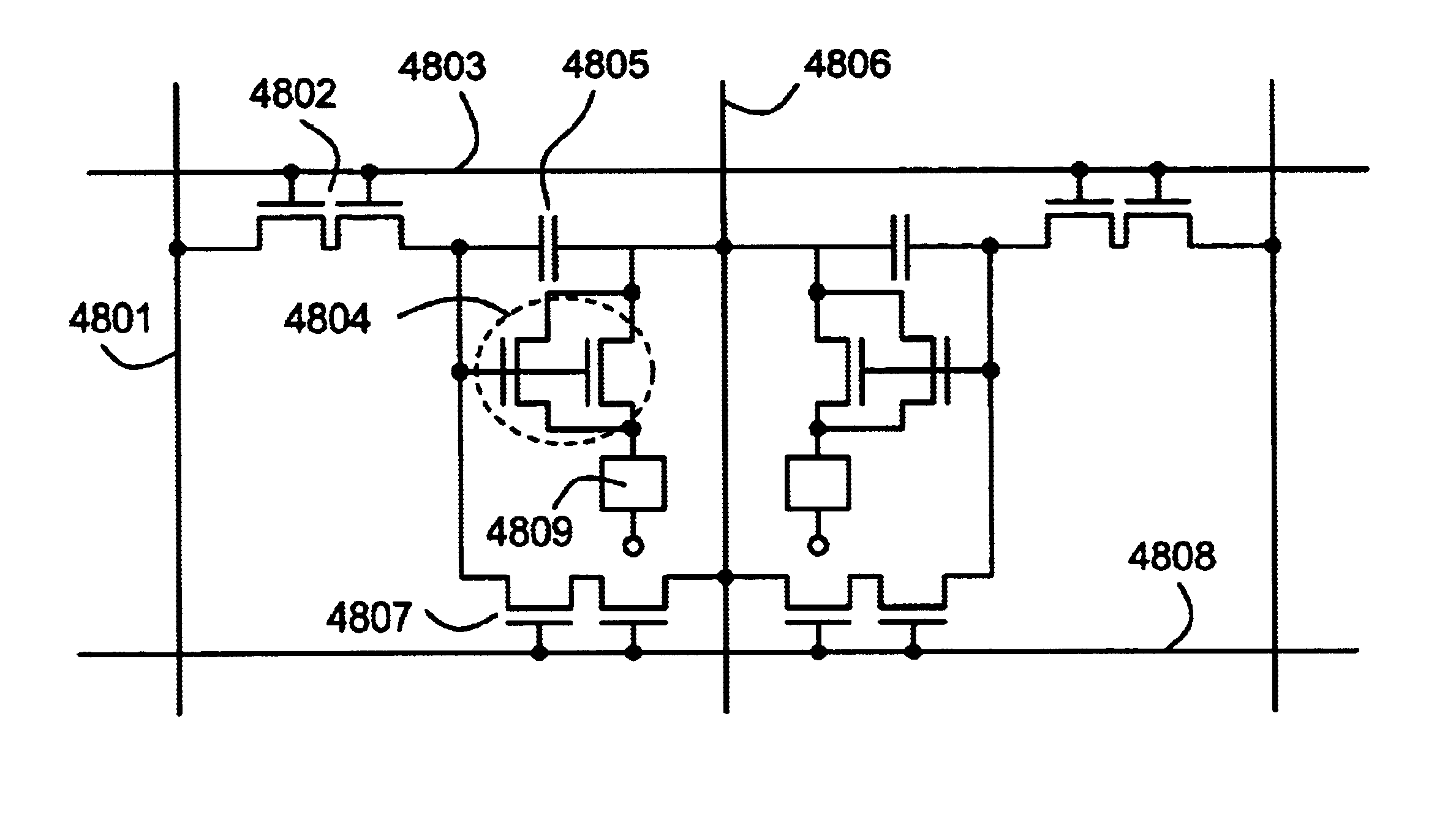
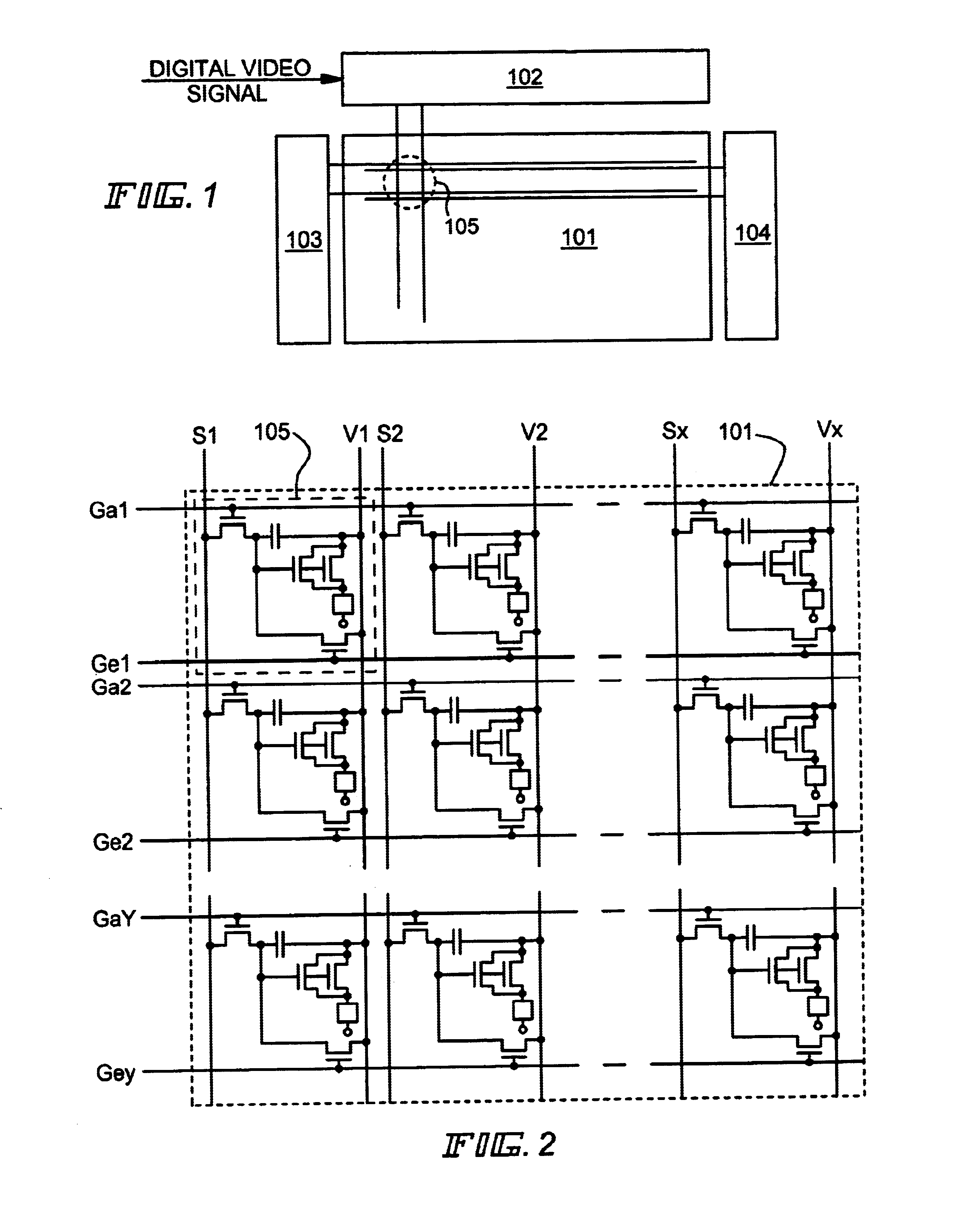
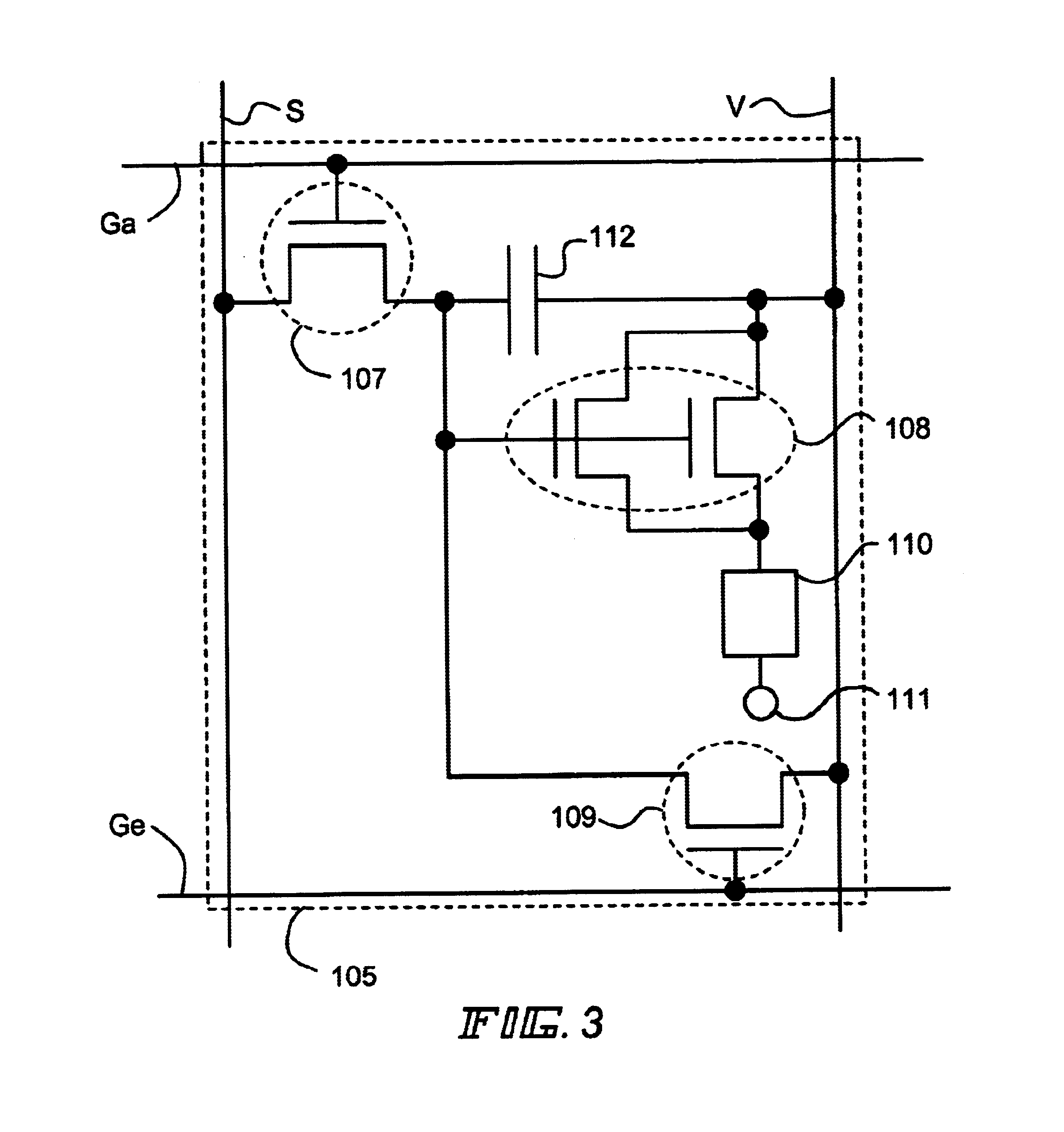
A case of performing 2.sup.6 gray scale display with a 6-bit digital video signal in an EL display according to the present invention is explained in Embodiment 1 using FIG. 5. Note that the EL display of Embodiment 1 has the structure shown in FIGS. 1 to 3.
First, the write in gate signal line Ga1 is selected in accordance with a write in gate signal input to the write in gate signal line Ga1 from the write in gate signal line driver circuit 103. The switching TFTs 107, all pixels (the first line of pixels) connected to the write in gate signal line Ga1 are then made an ON state.
At the same time, the first bit of a digital video signal is input to the source signal lines S1 to Sx from the source signal line driver circuit 102, and is input to the gate electrodes of the EL driver TFTs 108 through the switching TFTs 107.
When the digital video signal has "0" information, the EL driver TFTs 108 are made an OFF state in Embodiment 1. The power source electric potential is therefore not i...
embodiment 2
The order of appearance of the display periods Tr1 to Tr6 in a driving method of the present invention corresponding to a 6-bit digital video signal is explained in Embodiment 2.
FIG. 6 shows a timing chart of the driving method of Embodiment 2. Embodiment 1 may be referred to for detailed drive of the pixels, and therefore the explanation is omitted here. The longest non-display period (Td1 in Embodiment 2) within one frame period is provided at the end of the one frame period in the driving method of Embodiment 2. It appears to human eyes that there is a separation between the non-display period Td1 and the first display period (Tr4 in Embodiment 2) of the next frame period in accordance with the above structure. Unevenness of display, which occurs due to adjoining display periods for emitting light between adjacent frame periods, can thus be made more difficult for human eyes to recognize.
Note that, although a case for a 6-bit digital video signal is explained in Embodiment 2, the...
embodiment 3
A case of performing 2.sup.4 bit gray scale display with a 4-bit digital video signal in an EL display of the present invention is explained in Embodiment 3 using FIG. 7. Note that the EL display of Embodiment 3 has the structure shown in FIGS. 1 to 3.
First, the write in gate signal line Ga1 is selected in accordance with a write in gate signal input to the write in gate signal line Ga1 from the write in gate signal line driver circuit 103. The switching TFTs 107, all pixels (the first line of pixels) connected to the write in gate signal line Ga1 are then made an ON state.
At the same time, the first bit of a digital video signal is input to the source signal lines S1 to Sx from the source signal line driver circuit 102. The digital video signal is input to the gate electrodes of the EL driver TFTs 108 through the switching TFTs 107.
When the digital video signal has "0" information, the EL driver TFTs 108 are made an OFF state in Embodiment 3. The power source electric potential is ...
PUM
 Abstract
Description
Claims
Application Information