Optimization of die placement on wafers

a technology of dies and wafers, applied in semiconductor/solid-state device testing/measurement, instruments, photomechanical equipment, etc., can solve the problems of large increases in fabrication costs, increase in equipment costs, and reduce the yield of dies placed on the wafers

Inactive Publication Date: 2004-11-30
PDF SOLUTIONS INC
View PDF9 Cites 214 Cited by
  • Summary
  • Abstract
  • Description
  • Claims
  • Application Information

AI Technical Summary

Benefits of technology

Another object of the invention is place fields on the wafer in a way that maximizes the product reliability produced by the FAB.
A further object of the invention is to define the die shape and the reticle shape to maximize product reliability, FAB profitability and productivity.

Problems solved by technology

Large increases in fabrication cost are primarily driven by an increase in equipment costs.
Prior approaches to laying out dies on a wafer typically assume uniform manufacturing cost for placing reticles on the wafer.
Furthermore, new process technologies require that fields be printed on a wafer, even if they will not produce any good-yielding dies.
However, by doing so they will reduce the yield of the dies placed on the wafer.
Using the prior approaches will thus cause loss in yield, product reliability, FAB throughput and FAB profitability.

Method used


Image

  • Optimization of die placement on wafers
  • Optimization of die placement on wafers

Examples


Embodiment Construction

Detailed descriptions of preferred embodiments of the invention are provided herein. It is to be understood, however, that the present invention may be embodied in various forms. Therefore, specific details disclosed herein are not to be interpreted as limiting, but rather as a basis for the claims below and as a representative basis for teaching one skilled in the art to employ the present invention in virtually any appropriately detailed system, structure or manner.

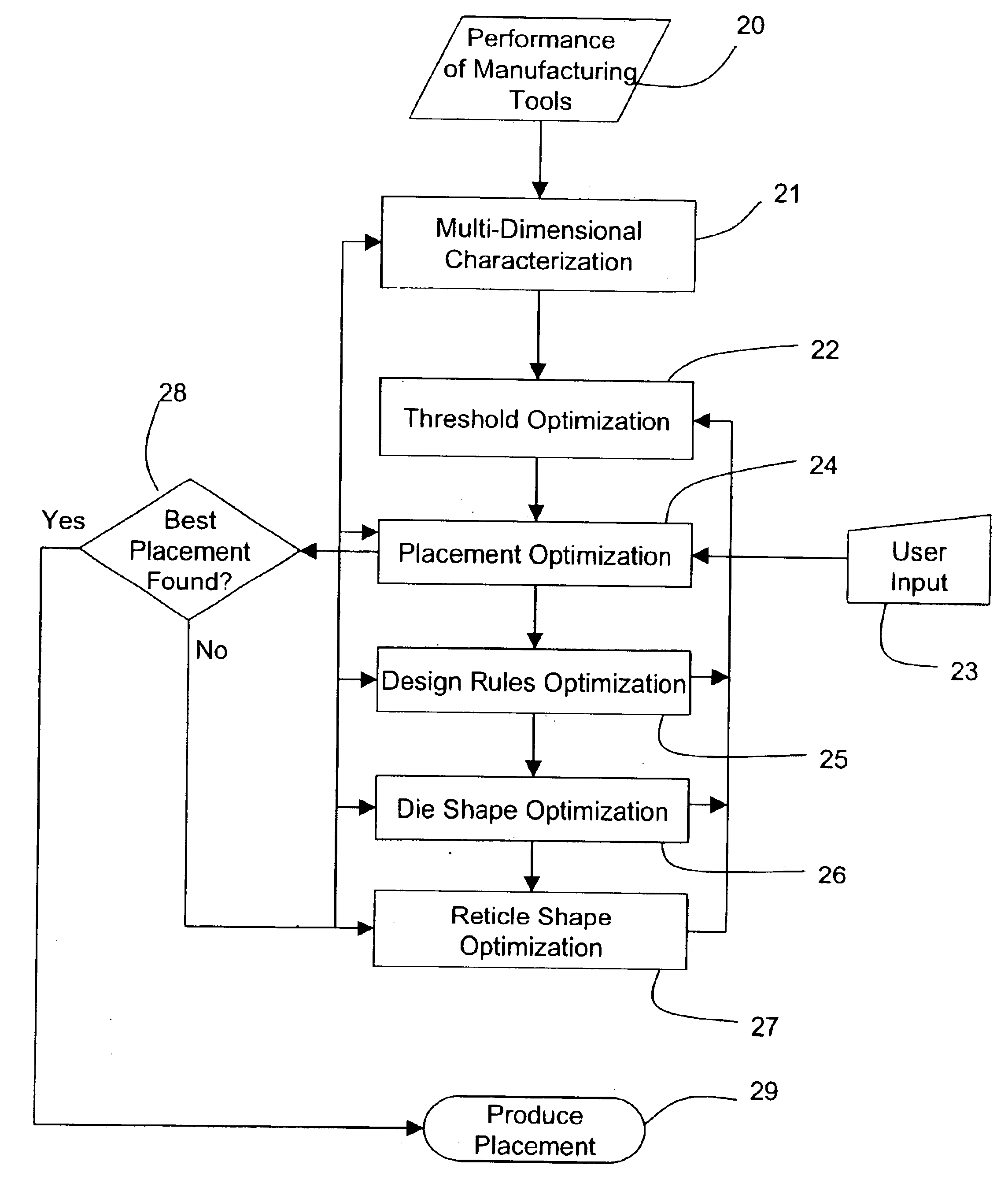
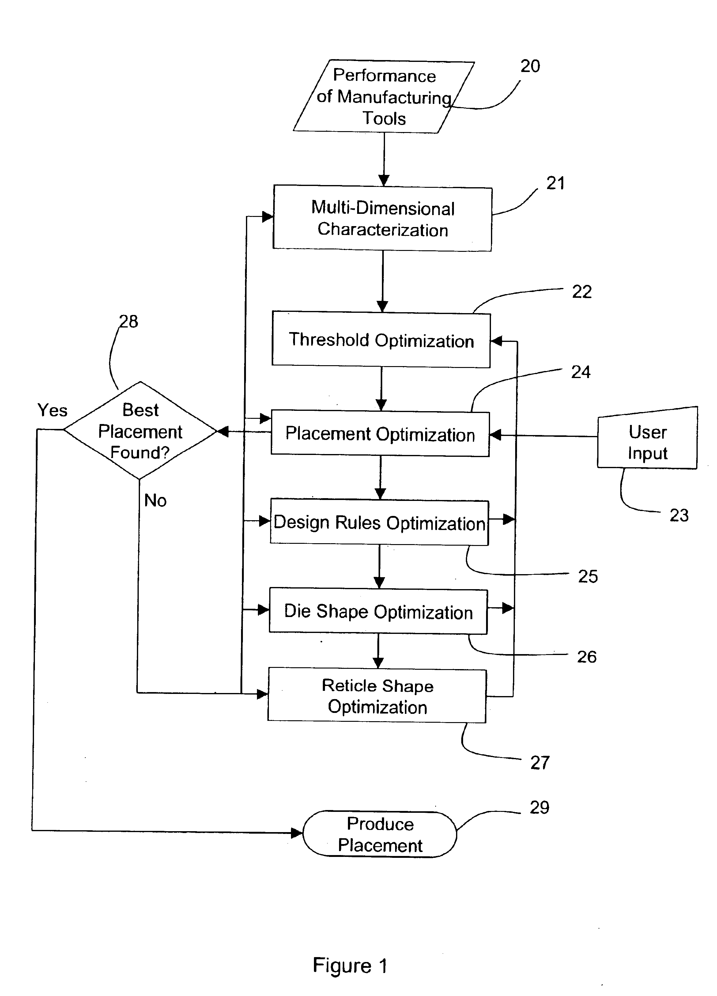
FIG. 1 shows a flow chart depicting an embodiment of the inventive process. The process begins in Step (20) with characterization of manufacturing tools. Such manufacturing tools include any or all processes and equipment used on a particular wafer of interest. In particular, Step (20) may involve characterizing different FAB equipment and processes in terms of their impact on, for example, yield, product performance, throughput, manufacturing and test, defect density analysis results, and reliability. This may be done,...


PUM

PropertyMeasurementUnit
yield threshold numberaaaaaaaaaa
yield thresholdaaaaaaaaaa
aspect ratiosaaaaaaaaaa

Abstract

A method of optimizing production of semiconductor devices on a wafer comprises steps of characterizing at least one effect of at least one manufacturing component on at least one optimization criterion; inputting user optimization data; and, based on the at least one effect and the user optimization data, performing optimization to determine a layout of semiconductor devices on the wafer that optimizes performance according to the user optimization data.

Description

1. Field of the InventionThis invention relates generally to the field of manufacturing of semiconductor devices, and more specifically to a process to print fields on a wafer in a way that increases the semiconductor manufacturer (FAB) throughput, profitability and / or product reliability.2. Background ArtThe annual sales of the semiconductor industry are around $152,000,000,000 to $200,000,000,000 a year. New semiconductor manufacturing plants (FABs) cost from $2 billion to more than $10 billion. Large increases in fabrication cost are primarily driven by an increase in equipment costs. Algorithms that increase a FAB's productivity and / or profitability, even by a small percentage, will reduce the cost of a die and will significantly increases the profitability of the semiconductor company.Today the following model is typically used to calculate the cost of a die:C.sub.die =C.sub.wafer / (N.sub.dies on a wafer *Y.sub.wafer)where:C.sub.die is the cost of a die;C.sub.wafer is the cost ...

Claims


Application Information

Patent Timeline
Patent Type & Authority Patents(United States)
IPC IPC(8): G03F7/20H01L21/66
CPCH01L22/20G03F7/70433
Inventor CADOURI, EITAN
Owner PDF SOLUTIONS INC
Why Eureka
Try Eureka