Method of manufacturing organic EL element, organic EL element, and organic EL display device

a technology of organic electroluminescent elements and display devices, which is applied in the direction of discharge tube luminescence screens, identification means, instruments, etc., can solve the problems of inability to say that the method is an efficient method of manufacturing elements, difficult to carry out patterning with high precision, and long time, etc., to achieve easy and precise patterning, excellent luminescence characteristics, and simple method

Inactive Publication Date: 2005-01-04
SEIKO EPSON CORP
View PDF119 Cites 76 Cited by
  • Summary
  • Abstract
  • Description
  • Claims
  • Application Information

AI Technical Summary

Benefits of technology

It is an object of the present invention to provide a method of manufacturing an organic EL element which makes it possible to carry out patterning easily and precisely, can attain optimization of a film design in a simple manner, and has excellent luminescence characteristics, as well as to provide an organic EL element and an organic EL display device.

Problems solved by technology

However, there is a problem in that a polymer or precursor that forms the organic luminescent layer lacks a sufficient resistance to a patterning process such as photolithography, so that it is very difficult to carry out patterning with highly precision.
Further, when several organic layers are to be formed by a vacuum deposition method, it takes a long time.
Therefore, such a method cannot be said to be an efficient method of manufacturing the element.

Method used


Image

  • Method of manufacturing organic EL element, organic EL element, and organic EL display device
  • Method of manufacturing organic EL element, organic EL element, and organic EL display device
  • Method of manufacturing organic EL element, organic EL element, and organic EL display device

Examples


second embodiment

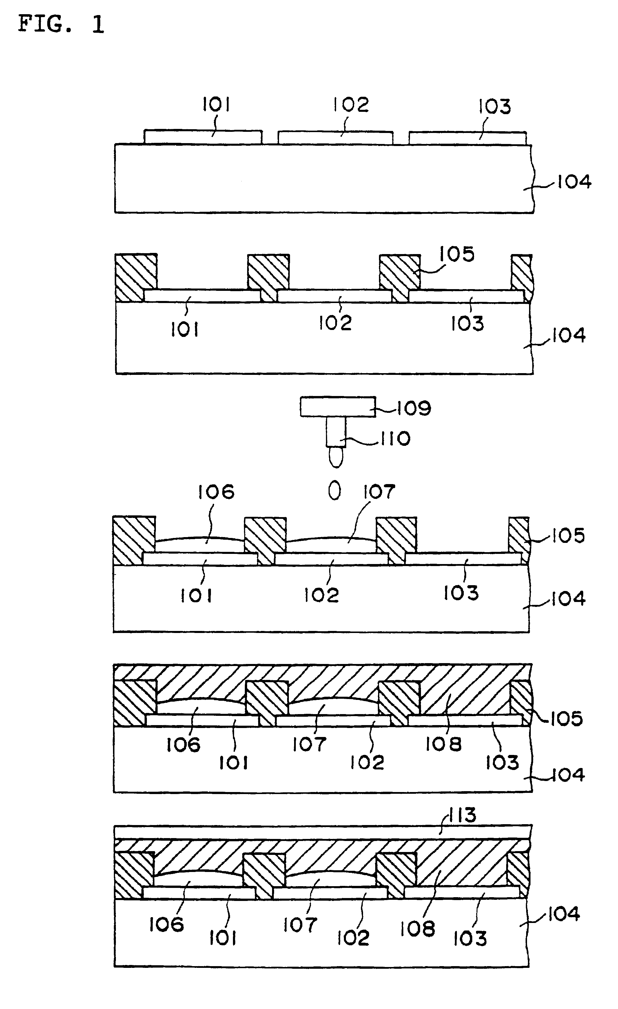
FIG. 2 shows the manufacturing method of the organic EL element according to the present invention.

In this second embodiment, after formation of pixel electrodes 201, 202 and 203 and banks 205 on a transparent substrate 204, a red luminescent layer 206 and a green luminescent layer 207 are formed by using an ink-jet method in the same manner as the first embodiment.

This second embodiment is different from the first embodiment in the point that a hole injection and transfer layer 208 is formed on the pixel electrode 203 and then a blue luminescent layer 210 is laminated on the layer 208. By the lamination of the hole injection and transfer layer 208 with the blue luminescent layer, it becomes possible to promote the injection and transfer of the holes from the electrode to improve the luminous efficiency as mentioned above.

Thus, in the manufacturing method for the organic EL element according to the present invention, it is preferable to laminate a hole injection and transfer layer w...

third embodiment

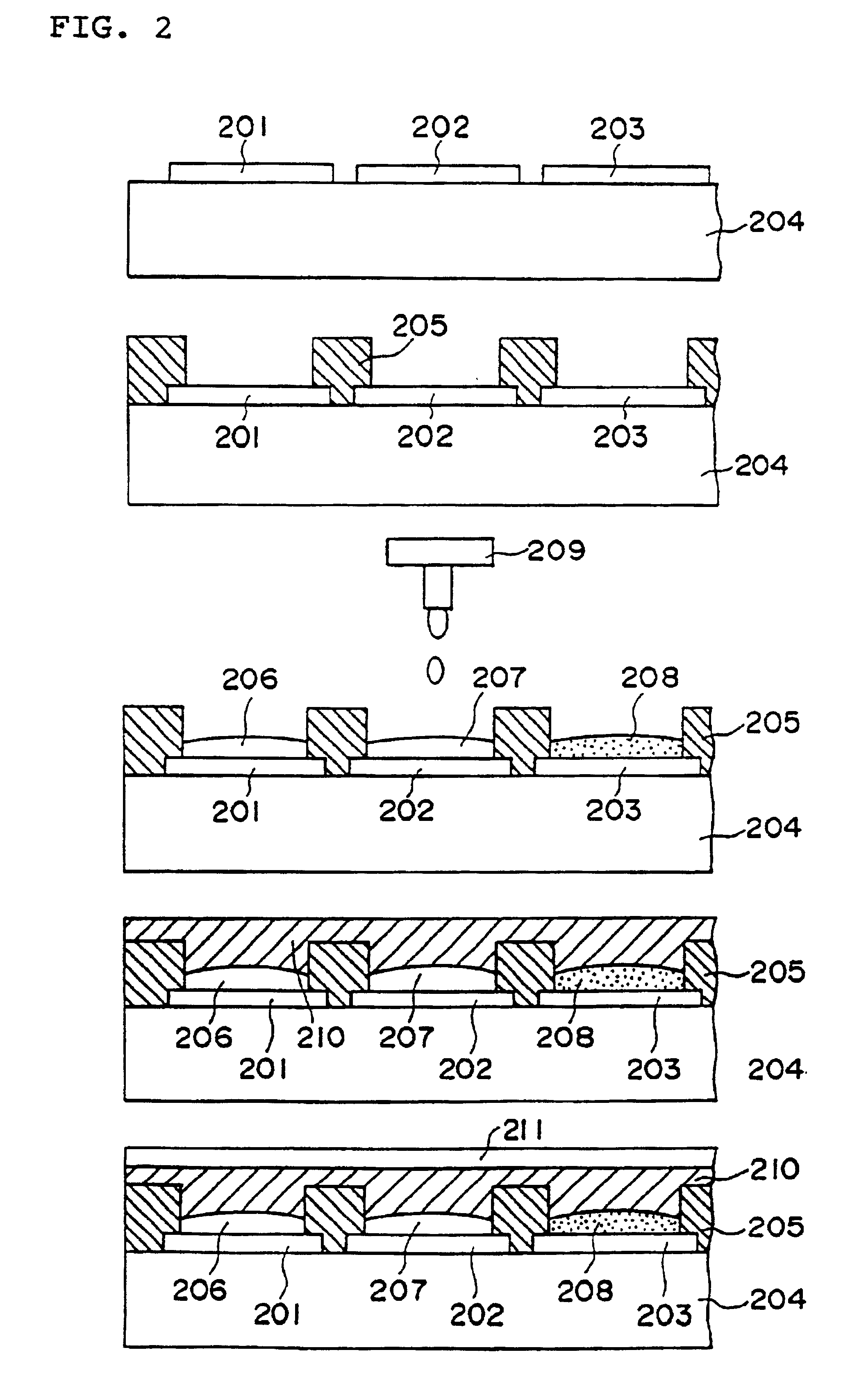
FIG. 3 shows the manufacturing method for the organic EL element according to the present invention.

In this third embodiment, after the formation of pixel electrodes 301, 302 and 303 and banks 305 on a transparent substrate 304, a red luminescent layer 306 and a green luminescent layer 307 are formed in the same manner as the first embodiment.

Next, a hole injection and transfer layer 308 is formed on the entire surface of the red luminescent layer 306, the green luminescent layer 307 and the pixel electrode 303. By laminating the hole injection and transfer layer 308 with the luminescent layers 306 and 307 in this way, it is possible to promote the injection and the transfer of the holes from the electrodes to improve the luminescence efficiency, as described in the above.

Further, by the same reason as in the above, it is preferable that the hole injection and transfer layer 308 is formed into a non-luminescent layer.

No particular limitation is imposed upon the forming method for th...

fourth embodiment

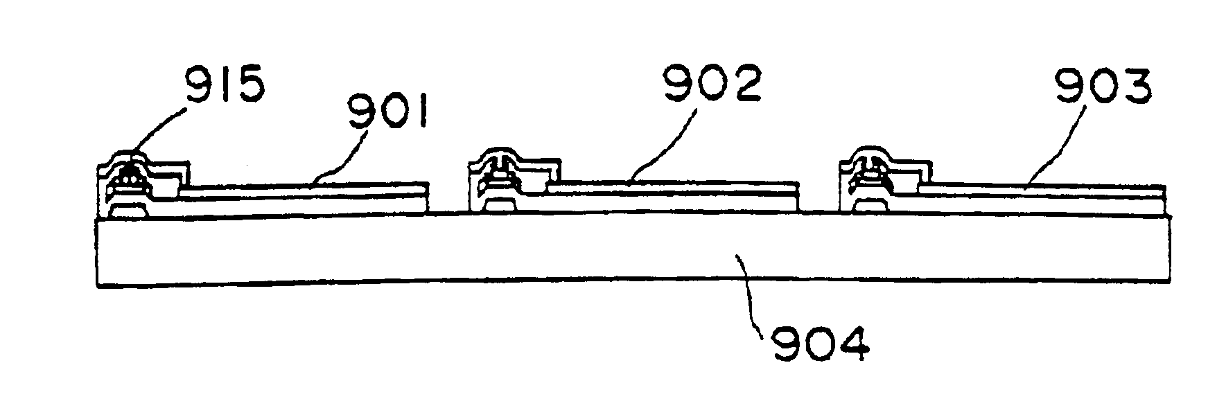
FIG. 4 shows the manufacturing method for the organic EL element according to the present invention.

In this fourth embodiment, after the formation of pixel electrodes 801, 802 and 803 and banks 805 on a transparent substrate 804 in the same way as the first embodiment, luminescent layers 806, 807 and 808 are patterned on the pixel electrodes 801, 802 and 803, respectively, by the ink-jet method. In this way, the amount of the material to be discharged for the respective luminescent layers, the number of times of the discharge and the formation pattern of the luminescent layers, for example, can be adjusted easily and handily, so that the luminescent characteristics and film thickness and the like of the respective luminescent layers can be controlled easily.

In addition, an electron injection and transfer layer 811 is formed on the luminescent layers 806, 807 and 808. The electron injection and transfer layer 811 facilitates the injection of the electrons from the cathode, and contri...


PUM

PropertyMeasurementUnit
contact angleaaaaaaaaaa

Abstract

A method of manufacturing an organic EL element according to the present invention comprises the steps of forming pixel electrodes (801), (802), (803) on a transparent substrate (804) and forming on the pixel electrodes by patterning luminescent layers (806), (807), (808) made of an organic compound by means of an ink-jet method. According to this method, it is possible to carry out a high precise patterning easily and in a short time, thereby enabling to carry out optimization for a film design and luminescent characteristic easily as well as making it easy to adjust a luminous efficiency.

Description

FIELD OF THE INVENTIONThe present invention relates to a method of manufacturing an organic electroluminescent (EL) element, an organic EL element, and an organic EL display device.BACKGROUND ARTAn organic EL element is an element which has a configuration in which a thin film containing a fluorescent organic compound is held between a cathode and an anode. In the organic EL element, electrons and holes are injected from the respective electrodes into the thin film to generate excitons through the recombimation of the electrons and holes. The organic EL element produces luminescence by utilizing emission of light (fluorescence or phosphorescence) at the deactivation of the excitons.The features of the organic EL element is that it is possible to obtain a high intensity surface luminescence on the order of 100 to 100,000 cd / m2 at a low voltage of less than 10V, and that it is possible to produce luminescence of from blue to red by the selection of the kind of fluorescent material.The...

Claims


Application Information

Patent Timeline
Patent Type & Authority Patents(United States)
IPC IPC(8): H01L27/32H01L27/28H01L51/50H01L51/52H05B33/10H01L51/40H01L51/56H01L51/05C09K11/00G09F9/30H01L51/00H05B33/12H05B33/22
CPCH01L27/3211H05B33/10H01L51/5237H01L27/3244H01L27/3281H01L27/3283H01L51/0005H01L51/001Y10T428/24868H01L51/56H01L27/3218Y10S428/917H01L51/5284Y10T428/10Y10T428/31855C09K2323/00H10K59/353H10K59/35H10K59/17H10K59/173H10K71/135H10K71/164H10K59/12H10K50/8426H10K50/865H10K50/844H10K71/00
Inventor MIYASHITA, SATORUKIGUCHI, HIROSHISHIMODA, TATSUYAKANBE, SADAO
Owner SEIKO EPSON CORP
Why Eureka
Try Eureka