
Method and apparatus for forming a planarizing pad having a film and texture elements for planarization of microelectronic substrates

Inactive Publication Date: 2005-01-04
MICRON TECH INC
View PDF159 Cites 6 Cited by
  • Summary
  • Abstract
  • Description
  • Claims
  • Application Information

AI Technical Summary

Benefits of technology

In one aspect of the invention, at least a portion of the planarizing medium material is in a liquid phase and separating the planarizing medium material includes forming discrete droplets of the planarizing medium material by mixing the planarizing medium material with a stream of gas. In another aspect of the invention, the discrete elements can be passed through apertures of a grate to control the distribution of the discrete elements on the support mate

Problems solved by technology

Yet, as the density of integrated circuits increases, it is necessary to have a planar substrate surface at several intermediate stages during the fabrication of devices on a substrate assembly because non-uniform substrate surfaces significantly increase the difficulty of forming sub-micron features.
For example, it is difficult to accurately focus photo patterns to within tolerances approaching 0.1 micron on non-uniform substrate surfaces because sub-micron photolithographic equipment generally has a very limited depth of field.
One drawback with the foregoing fabrication method is that the mold 50 may deform the texture elements 41 as the mold 50 is withdrawn from the planarizing pad 40.

Method used


Image

  • Method and apparatus for forming a planarizing pad having a film and texture elements for planarization of microelectronic substrates
  • Method and apparatus for forming a planarizing pad having a film and texture elements for planarization of microelectronic substrates
  • Method and apparatus for forming a planarizing pad having a film and texture elements for planarization of microelectronic substrates

Examples


Embodiment Construction

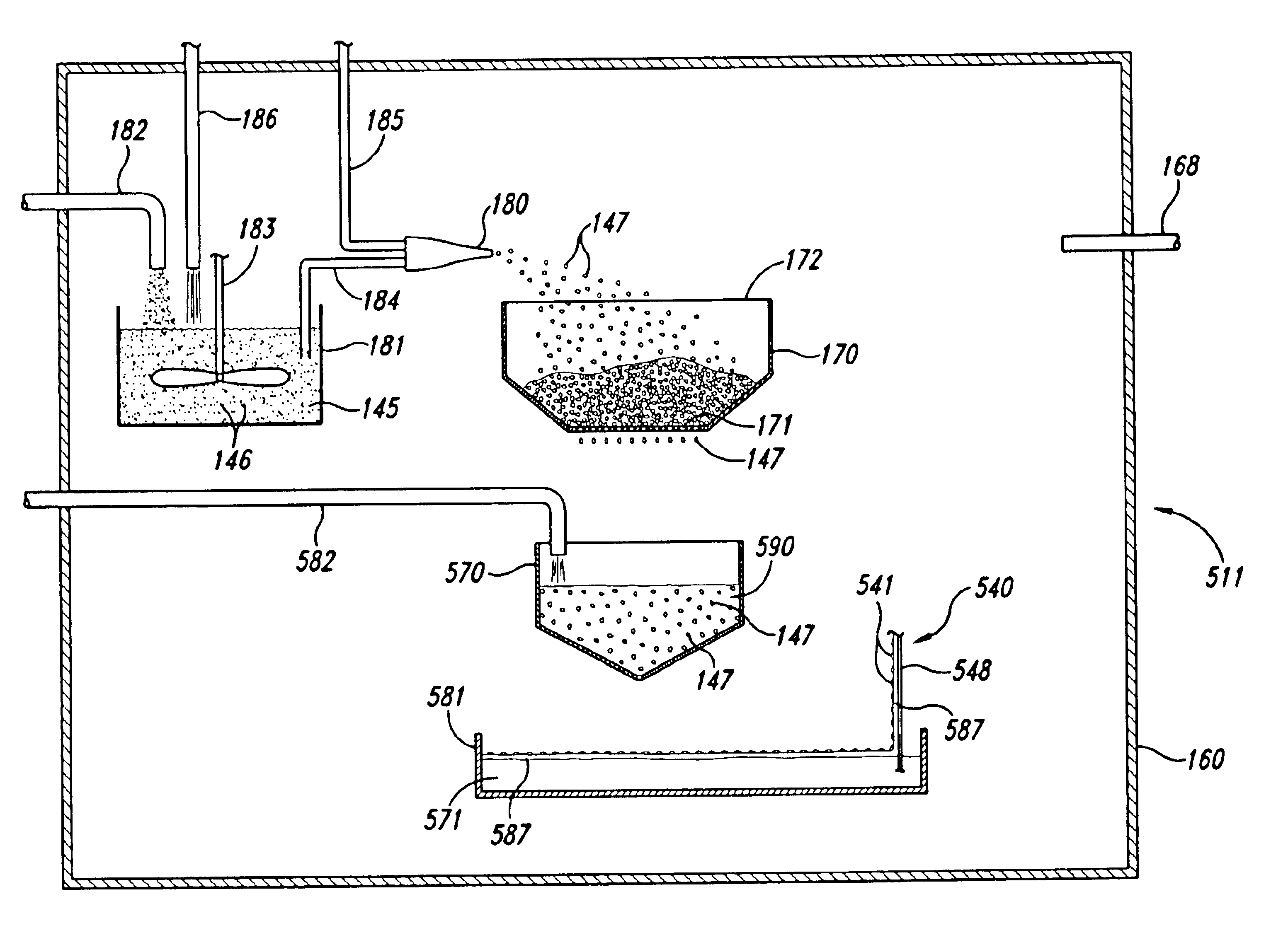
The present disclosure describes planarizing media and methods and apparatuses for forming planarizing media for chemical and / or chemical-mechanical planarizing of substrates and substrate assemblies used in the fabrication of microelectronic devices. Many specific details of certain embodiments of the invention are set forth in the following description and in FIGS. 3-6 to provide a thorough understanding of these embodiments. One skilled in the art, however, will understand that the present invention may have additional embodiments, or that the invention may be practiced without several of the details described below.

FIG. 3 is a partially schematic side elevational view of an apparatus 111 for forming a planarizing pad 140 from a planarizing pad material 145 in accordance with an embodiment of the invention. The apparatus 111 can include a nozzle 180 that separates the planarizing pad material 145 into discrete particles 147. The particles 147 collect in a hopper 170 that distribu...


PUM

PropertyMeasurementUnit
Fractionaaaaaaaaaa
Fractionaaaaaaaaaa
Lengthaaaaaaaaaa

Abstract

A planarizing pad for planarzing a microelectronic substrate, and a method and apparatus for forming the planarizing pad. In one embodiment, planarzing pad material is mixed with compressed gas to form a plurality of discrete elements that are distributed on a film support material. The film support material is supported by a liquid and is drawn from the liquid with a backing layer. At least a portion of the discrete elements are spaced apart from each other on the film support material to form a textured surface for engaging a microelectronic substrate and removing material from the microelectronic substrate. The discrete elements can be uniformly or randomly distributed on the film support material.

Description

TECHNICAL FIELDThis invention relates to planarizing pads and methods and apparatuses for forming planarizing pads for planarizing microelectronic substrates.BACKGROUND OF THE INVENTIONMechanical and chemical-mechanical planarization processes (collectively in “CMP”) are used in the manufacturing of electronic devices for forming a flat surface on semiconductor wafers, field emission displays and many other microelectronic-device substrate assemblies. CMP processes generally remove material from a substrate assembly to create a highly planar surface at a precise elevation in the layers of material on the substrate assembly. FIG. 1 schematically illustrates an existing web-format planarizing machine 10 for planarzing a substrate 12. The planarizing machine 10 has a support table 14 with a top-panel 16 at a workstation where an operative portion “A” of a planarizing pad 40 is positioned. The top-panel 16 is generally a rigid plate to provide a flat, solid surface to which a particular...

Claims


Application Information

Patent Timeline
IPC IPC(8): B24B49/00H01L21/302H01L21/02B24B37/24B24B37/26B24D13/14B24D18/00
CPCB24B37/24B24D18/00B24B37/26B24B37/245
Inventor MEIKLE, SCOTT G.
Owner MICRON TECH INC
Features
  • Generate Ideas
  • Intellectual Property
  • Life Sciences
  • Materials
  • Tech Scout
  • Unparalleled Data Quality
  • Higher Quality Content
  • 60% Fewer Hallucinations
Learn More