Level translator for high voltage digital CMOS process

a technology of digital cmos and translator, applied in logic circuits, logic circuit coupling/interface arrangements, pulse techniques, etc., can solve the problems that the level shifter b>100/b> works poorly in high-speed applications

Inactive Publication Date: 2005-01-04
NAT SEMICON CORP
View PDF10 Cites 99 Cited by
  • Summary
  • Abstract
  • Description
  • Claims
  • Application Information

AI Technical Summary

Benefits of technology

The present invention provides a high-speed level shifter. A level shifter in accordance with the present invention includes an input stage that receives a first s

Problems solved by technology

One limitation of level shifter 100 is that level s

Method used


Image

  • Level translator for high voltage digital CMOS process
  • Level translator for high voltage digital CMOS process
  • Level translator for high voltage digital CMOS process

Examples


Embodiment Construction

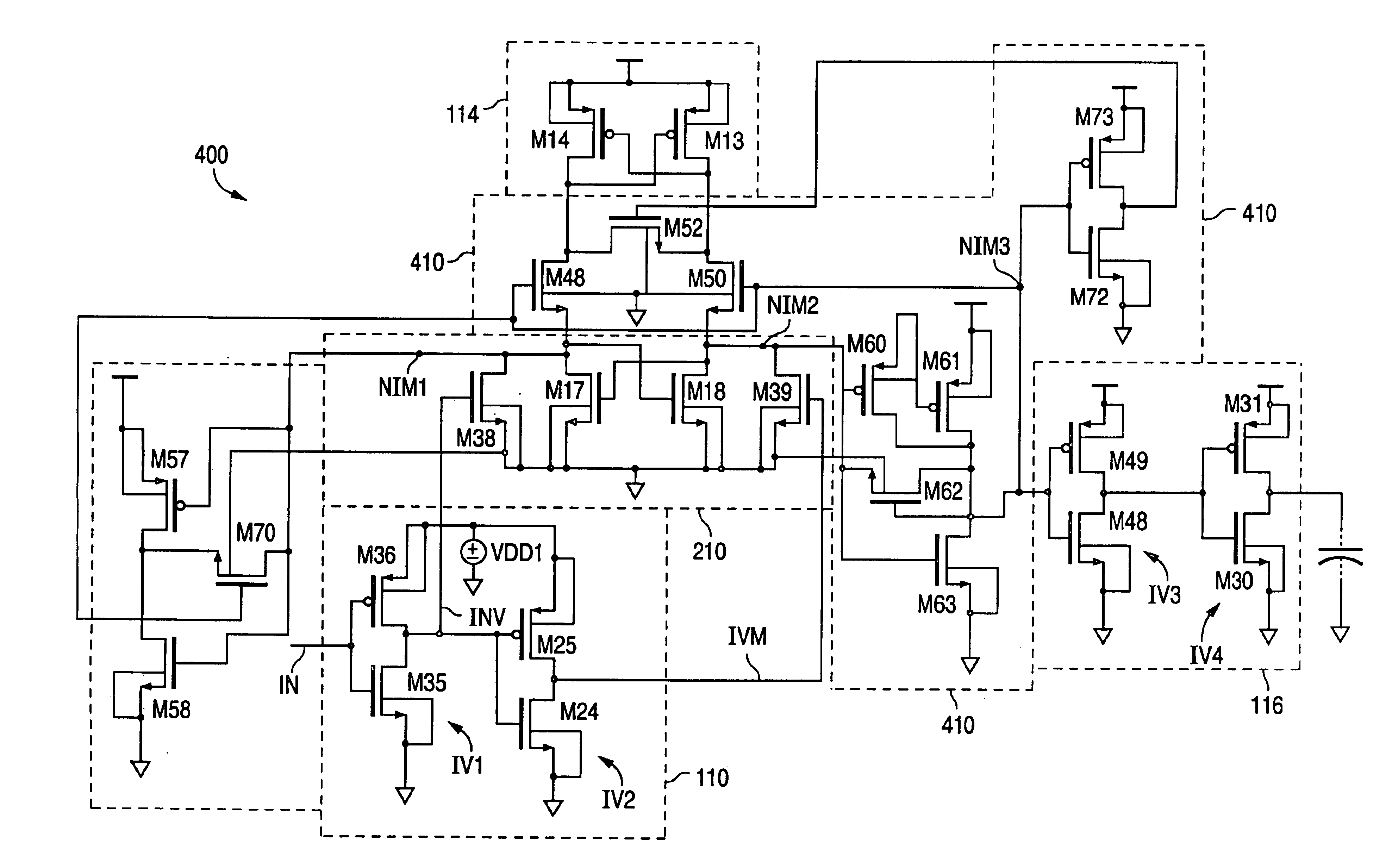
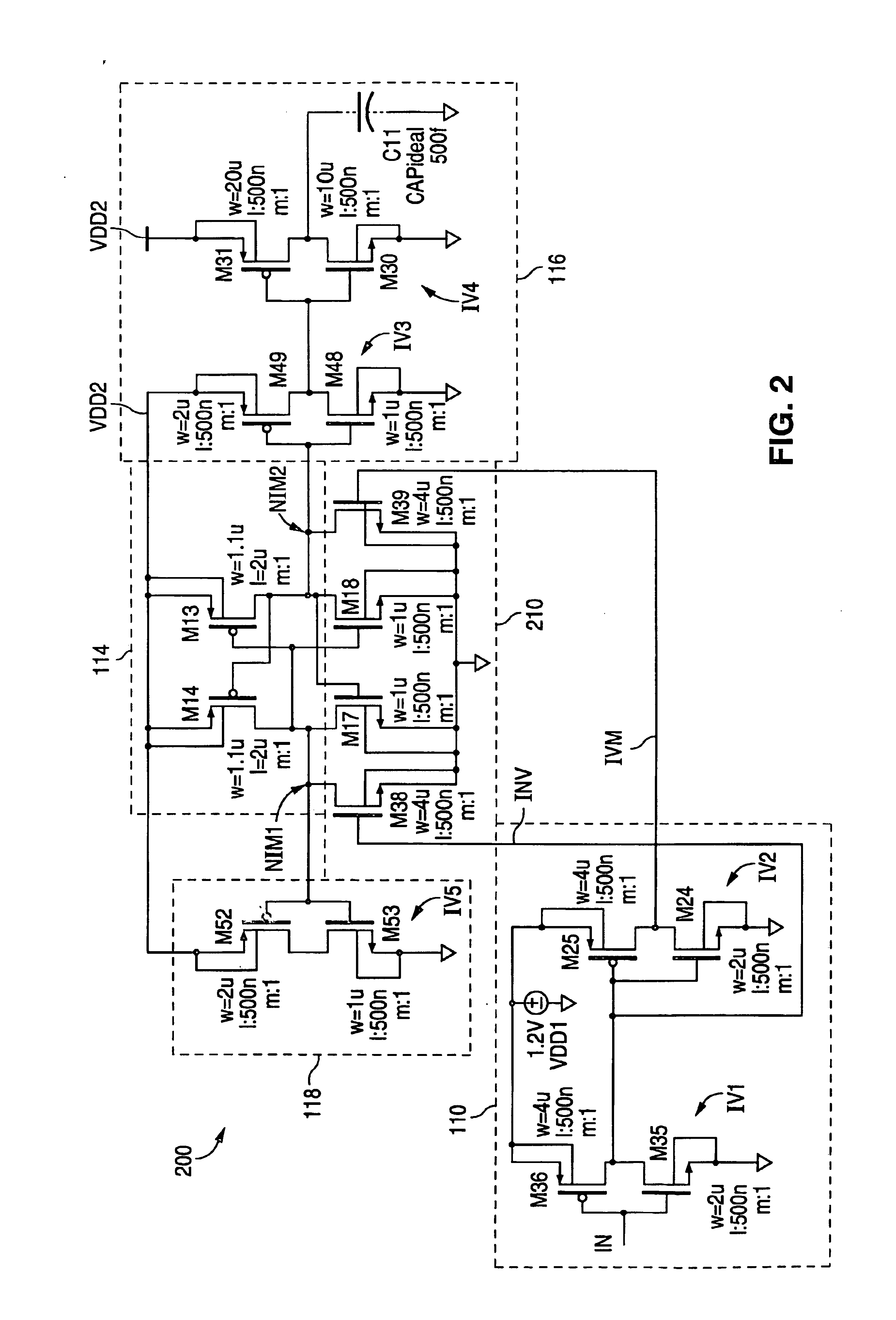
FIG. 2 shows a circuit diagram that illustrates an example of a level shifter 200 in accordance with the present invention. Level shifter 200 is similar to level shifter 100 and, as a result, utilizes the same reference numerals to designate the structures that are common to both level shifters.

As shown in FIG. 2, level shifter 200 differs from level shifter 100 in that level shifter 200 utilizes a pull down stage 210 in lieu of pull down stage 112. Pull down stage 210, which is connected to the first intermediate node NIM1 and the second intermediate node, pulls down the voltage on the first intermediate node NIM1 when the input digital voltage IN is in a first logic state, and pulls down the voltage on the second intermediate node NIM2 when the input voltage IN is in a second logic state.

Pull down stage 210 includes a NMOS transistor M38 and a NMOS transistor M39. NMOS transistor M38 has a source connected to ground, a drain connected to the first intermediate node NIM1, and a gat...


PUM


Abstract

The speed of a level shifter is increased by utilizing an additional transistor to pull down the voltage on a first intermediate node, and an additional transistor to pull down the voltage on a second intermediate node. In addition, a precharge circuit is utilized to precharge the voltage on the first and second intermediate nodes to further increase the speed of the level shifter.

Description

BACKGROUND OF THE INVENTION1. Field of the InventionThe present invention relates to level shifters and, more particularly, to a high-speed level shifter.2. Description of the Related ArtA level shifter is a common circuit device that is used to translate a voltage from a first voltage level to a second voltage level. For example, deep sub-micron digital circuits represent a logic one with a voltage of approximately 1.2 volts. When these circuits communicate with other circuits that represent a logic one with a voltage of approximately 3.6 volts, a level shifter is used to shift the 1.2 volt level to a 3.6 volt level.FIG. 1 shows a circuit diagram that illustrates an example of a prior art level shifter 100. As shown in FIG. 1, level shifter 100 includes an input stage 110 that receives an input digital signal IN, and outputs an inverted input signal INV and a non-inverted input signal IVM. Input stage 110 has a first inverter IV1 that inverts the input digital voltage IN and output...

Claims


Application Information

Patent Timeline
IPC IPC(8): H03K19/017H03K19/01
CPCH03K19/01721
Inventor DOYLE, JAMES THOMAS
Owner NAT SEMICON CORP
Why Eureka
Try Eureka