Dead Time Control

a control and dead time technology, applied in pulse manipulation, pulse technique, instruments, etc., can solve the problem of reducing the benefit of using the gan devi

Active Publication Date: 2016-09-22
PSEMI CORP
View PDF0 Cites 54 Cited by
  • Summary
  • Abstract
  • Description
  • Claims
  • Application Information

AI Technical Summary

Benefits of technology

[0006]According to a first aspect of the present disclosure, a circuital arrangement is presented, the circuital arrangement being configured to control a high side (HS) device and a low side (LS) device arranged in a stacked configuration, the HS device and the LS device capable of withstanding a voltage higher than or equal to a first voltage, the circuital arrangement comprising: a HS control circuit operating between a first switching voltage and a second switching voltage based on the first switching voltage, the first switching voltage being an output voltage at a common output node of the stacked HS device and LS device, the HS control circuit configured to provide a HS output control signal at a voltage higher than the first voltage to the HS device; a LS control circuit configured to provide a LS output control signal to the LS device; and a dead time control circuit configured, to generate timing information for the HS output control signal and the LS output control signal, wherein all transistor devices of the HS control circuit, the LS control circuit and the dead time controller circuit, are each configured to withstand a second voltage substantially smaller than the first voltage.
[0007]According to a second aspect of the present disclosure, a method for controlling a high side (HS) device and a low side (LS) device arranged in a stacked configuration is presented, the HS device and the LS device capable of withstanding a voltage higher than or equal to a first voltage, the method comprising: receiving an input timing signal; based on the receiving, generating control timing signals for controlling the HS device and the LS device; generating, via capacitve coupling of the control timing signals, an HS output control signal at a voltage higher than the first voltage; generating, based on the control timing signals, an LS output control signal; controlling the HS device via the HS output control signal; and controlling the LS device via the LS output control signal; wherein the steps of generating are provided by transistor devices configured to withstand a second voltage substantially smaller than the first voltage.

Problems solved by technology

Since these control transistors typically have poor figure of merit (FOM), compared to the FOM of the GaN devices, which can thereby, for example, limit the operating frequencies of the GaN devices, the overall circuit (e.g. power management) can be limited in performance by the large, high voltage control transistors which can be difficult to charge and discharge quickly (e.g. their FOM is too high) and therefore the benefit of using the GaN devices can be substantially reduced.

Method used


Image

  • Dead Time Control
  • Dead Time Control
  • Dead Time Control

Examples


Embodiment Construction

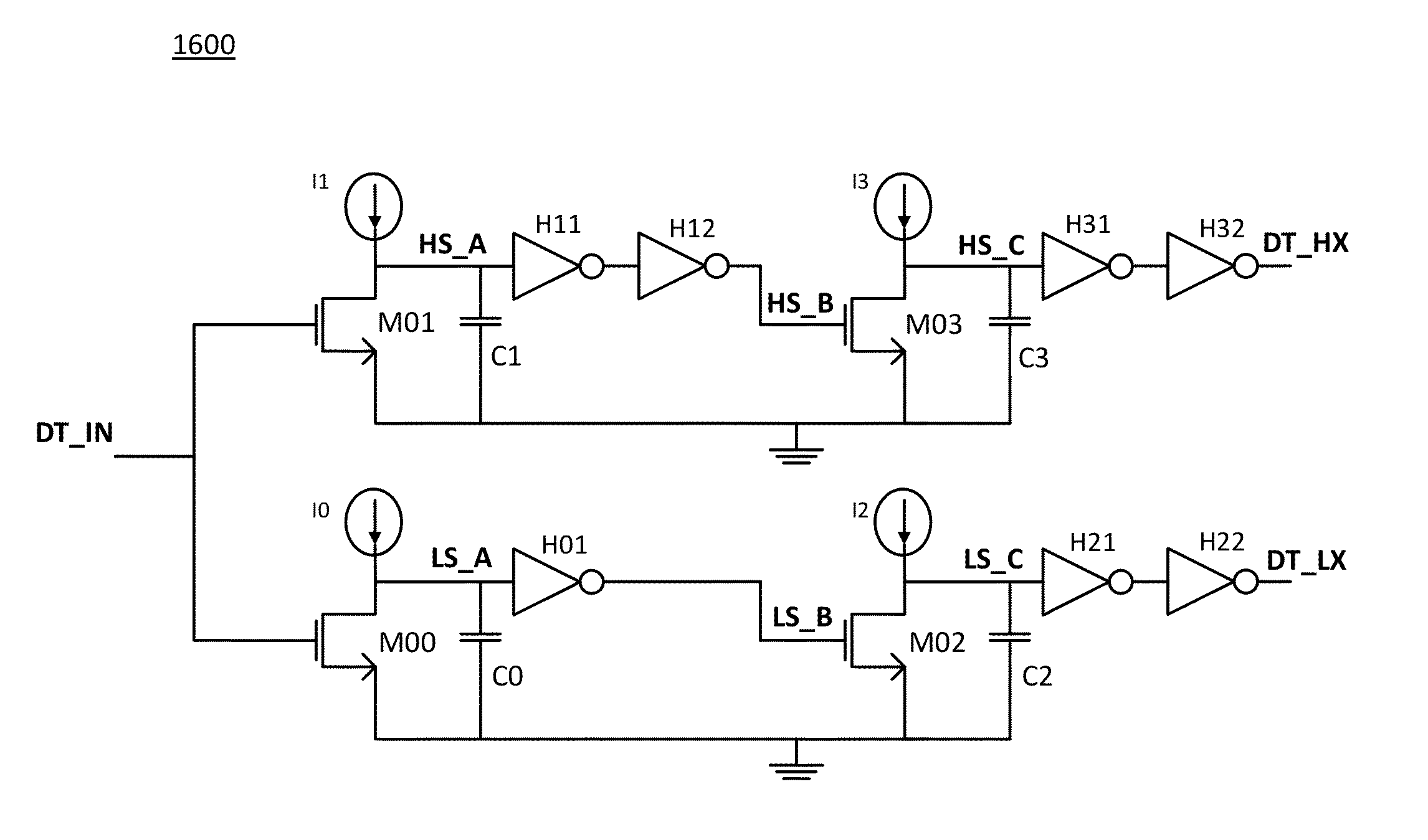
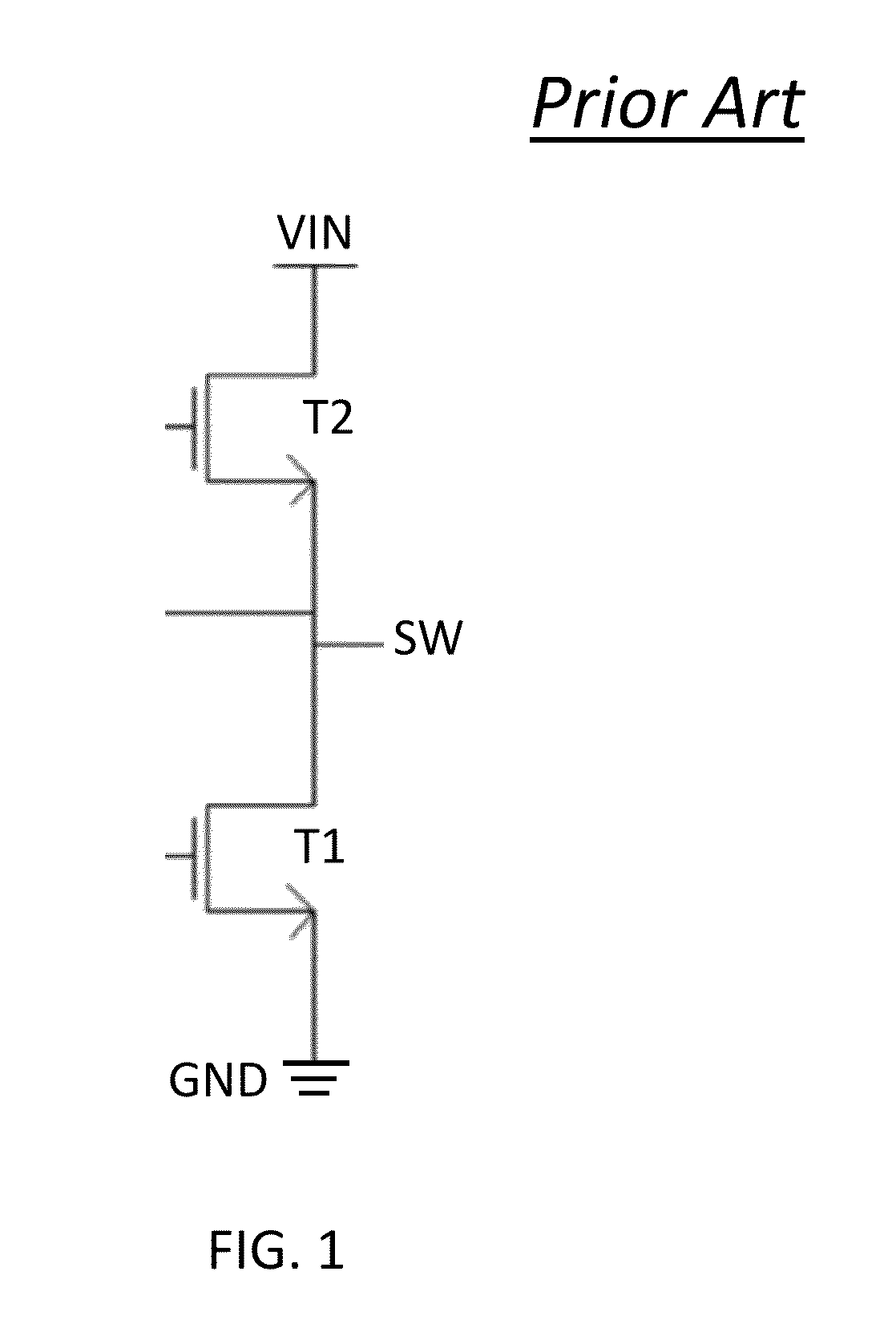
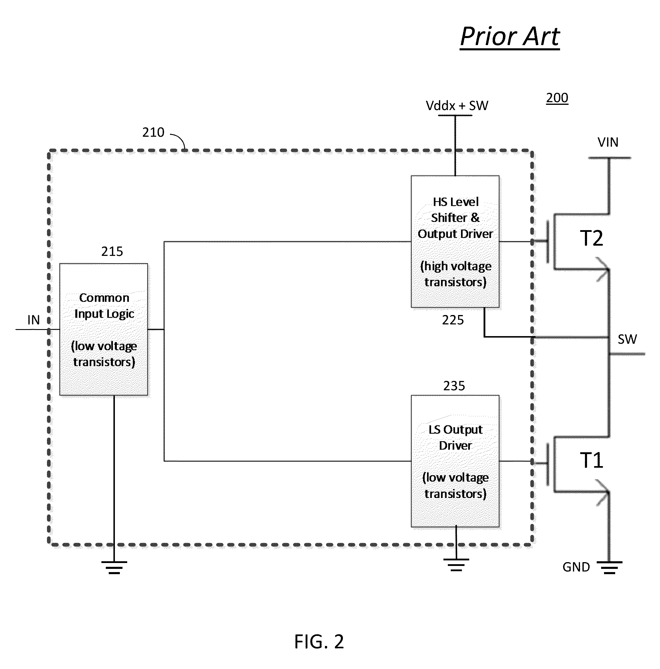
[0035]It can be desirable to use small, low breakdown voltage MOSFET transistors which can have figure of merits (FOMs), as measured, for example, by the product of the ON resistance Ron of the transistor and the gate charge Cg of the transistor, similar to or better (lower) than the FOM of high voltage transistors (transistors with higher breakdown voltage) as controlling transistors in applications where high voltage semiconductor devices operating in high voltage conditions are controlled. Such MOSFETs can allow for best use of the GaN characteristics, thereby improving both performance and cost of the implementation. In addition, by implementing a single chip silicon on insulator (SOI) MOSFET solution based on low voltage MOSFETs, additional functionality can be included which address additional areas known to a person of ordinary skill in the art such as, but not limited to, GaN gate voltage overdrive protection, minimum gate drive requirements, dead time control, temperature s...


PUM


Abstract

Systems, methods, and apparatus for use in biasing and driving high voltage semiconductor devices using only low voltage transistors are described. The apparatus and method are adapted to control multiple high voltage semiconductor devices to enable high voltage power control, such as power amplifiers, power management and conversion and other applications wherein a first voltage is large compared to the maximum voltage handling of the low voltage control transistors. Timing of control signals can be adjusted via internal and/or external components so as to minimize shoot trough currents in the high voltage devices. A DC/DC power conversion implementation from high input voltage to low output voltage using a novel level shifter which uses only low voltage transistors is also provided. Also presented is a level shifter in which floating nodes and high voltage capacitive coupling and control enable the high voltage control with low voltage transistors.

Description

CROSS REFERENCE TO RELATED APPLICATIONS[0001]This application is a continuation-in-part of commonly owned and co-pending U.S. patent application Ser. No. 14 / 661,848 filed Mar. 18, 2015, entitled “Level Shifter”, the disclosure of which is incorporated herein by reference in its entirety. The present application may be related to U.S. Pat. No. 5,416,043, issued on May 6, 1995 and entitled “Minimum charge FET fabricated on an ultrathin silicon on sapphire wafer”, the disclosure of which is incorporated herein by reference in its entirety. The present application may also be related to U.S. Pat. No. 5,600,169, issued on Feb. 4, 1997 and entitled “Minimum charge FET fabricated on an ultrathin silicon on sapphire wafer”, the disclosure of which is incorporated herein by reference in its entirety. The present application may also be related to PCT publication number WO2009 / 108391 entitled “Method and Apparatus for use in Digitally Tuning a Capacitor in an Integrated Circuit Device”, publi...

Claims


Application Information

Patent Timeline
Patent Type & Authority Applications(United States)
IPC IPC(8): H03K5/14H03K5/1534H02M3/158H03K3/356
CPCH03K5/14H03K3/356104H03K2005/00019H02M3/158H03K5/1534H02M1/38H02M7/538H03K17/689H03K19/018514
Inventor ABESINGHA, BUDDHIKAGREEN, MERLIN
Owner PSEMI CORP
Why Eureka
Try Eureka