Level shifter with reduced duty cycle variation

a level shifter and duty cycle technology, applied in the field of electronic circuits, can solve problems such as excessive gate-to-drain voltage, inability to operate at optimal speed, and reliability problems of the transistor

Inactive Publication Date: 2005-12-29
FREESCALE SEMICON INC
View PDF11 Cites 55 Cited by
  • Summary
  • Abstract
  • Description
  • Claims
  • Application Information

AI Technical Summary

Problems solved by technology

Because the gate oxides of these N-channel transistors are thin relative to transistor oxides in the peripheral circuitry, a floating drain voltage causes transistor reliability problems such as hot carrier injection (HCI), an excessi...

Method used


Image

  • Level shifter with reduced duty cycle variation
  • Level shifter with reduced duty cycle variation
  • Level shifter with reduced duty cycle variation

Examples


Embodiment Construction

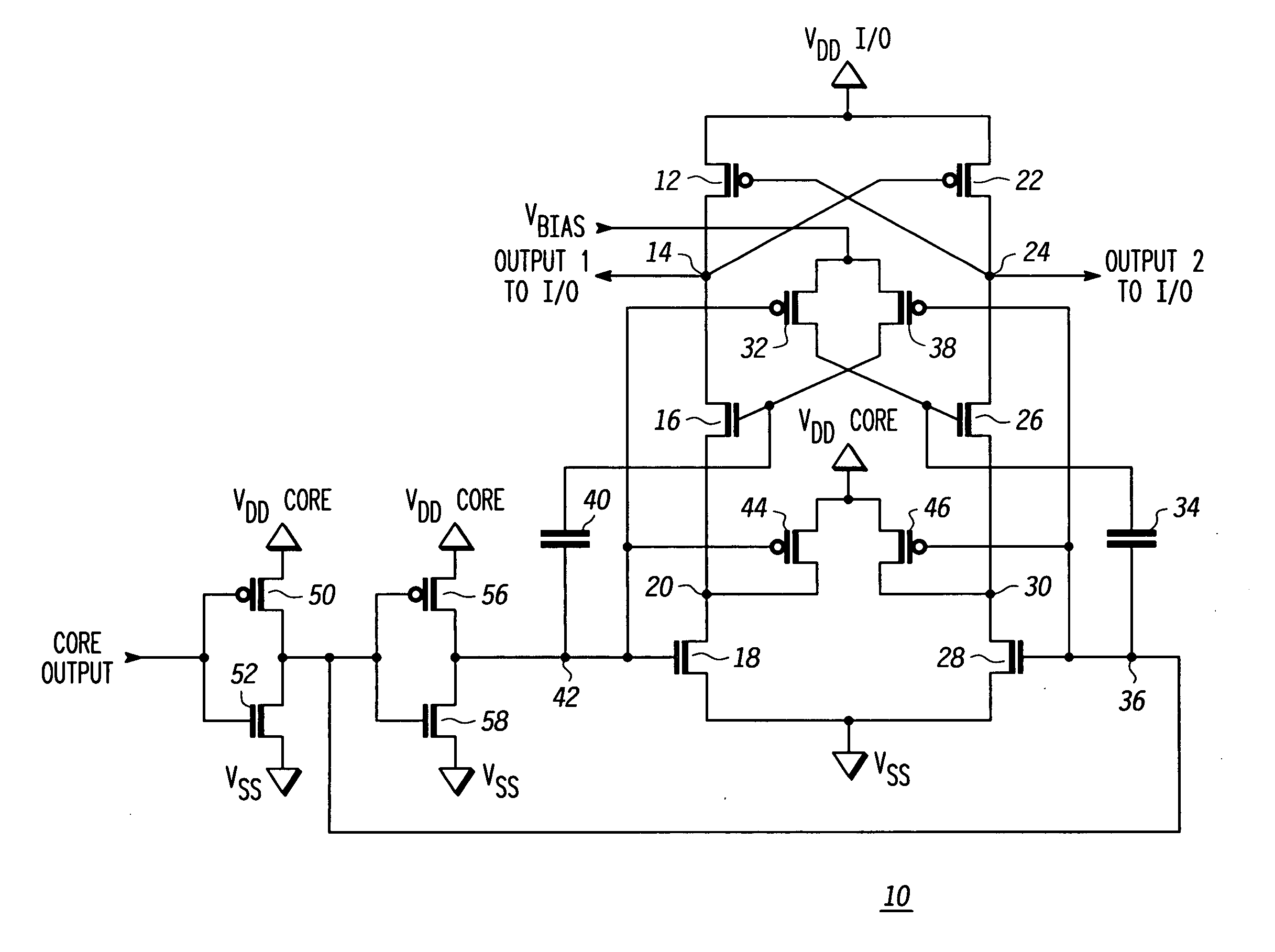
[0008]FIG. 1 illustrates a voltage level shifter 10 for shifting a voltage from core circuitry (not shown) up to a higher value for use by I / O circuitry (not shown). A P-channel transistor 12 has a source connected to an I / O power supply labeled VDDI / O. A drain of transistor 12 is connected at a node 14 to a drain of an N-channel transistor 16. A gate of transistor 12 is connected to a node 24. In the illustrated form transistors in the I / O circuitry have gate oxide thickness that are much greater than transistors in the core. The transistors with large gate oxide thickness are referred to herein as ‘high voltage’ transistors and the transistors with smaller gate oxide thickness are referred to herein as ‘low voltage’ transistors. Transistor 16 has a source connected to a drain of an N-channel transistor 18 at a node 20. A source of transistor 18 is connected to a power supply voltage terminal labeled VSS. The VSS supply is typically an earth ground potential, but regardless of what...


PUM


Abstract

A voltage level shifting circuit (10) transitions an input signal at a first voltage to a second voltage higher than the first voltage. A cross-coupled latch provides the second voltage. Cascode configured transistors (16, 26) are connected in series with input transistors (18, 28) that receive the first voltage in complementary form. Capacitive devices (34, 40) are connected between the first voltage and gates of the cascode configured transistors for allowing independent small signal variations to occur on the gates of the cascode configured transistors for better control of duty cycle and rise and fall time matching of the level shifting circuit. Isolation devices (32, 38) permit independent modification of small signal voltages to occur on the gates of the cascode configured transistors.

Description

FIELD OF THE INVENTION [0001] This invention relates to electronic circuits, and more particularly to electronic circuitry for shifting a voltage level of a signal. BACKGROUND OF THE INVENTION [0002] Integrated circuits typically have peripheral or input / output (I / O) circuitry and internal core circuitry. The cores of the integrated circuit perform various processing-specific functions and are desired to operate as fast as possible with minimal power consumption. As a result, power supply voltages that are used to power the core circuitry have been getting smaller with the enhancement of semiconductor processing. The I / O circuitry however functions to provide circuit drive strength to drive or provide signals from the core to external sources at a specified signal power. The I / O circuitry also is frequently required to interface with various interface standards. Such interface standards have not been getting smaller in voltage value to the same degree that core circuitry has been. A...

Claims


Application Information

Patent Timeline
IPC IPC(8): H03F1/26H03K25/02
CPCH03K25/02
Inventor SCHULMEYER, KYLE C.MATTHEWS, LLOYD P.PAPPERT, BERNARD J.
Owner FREESCALE SEMICON INC
Why Eureka
Try Eureka