Boost-biased level shifter

a level shifter and bias technology, applied in the field of digital circuits, can solve the problems of occupying more space, reducing the performance of the core cmos, and reducing the production cost, so as to achieve the effect of improving performan

Active Publication Date: 2006-12-19
TAIWAN SEMICON MFG CO LTD
View PDF21 Cites 52 Cited by
  • Summary
  • Abstract
  • Description
  • Claims
  • Application Information

AI Technical Summary

Benefits of technology

[0011]In another aspect of the preferred embodiment, a fail proof circuit is added. The fail proof circuit comprises a pair of thick oxide nMOS transistors having their gates coupled to the input signal and the inverted input signal and their drains coupled to the output node and a complementary node of the output node. The fail proof circuit works in parallel with the input receiver circuit and the voltage divider circuit. It prevents the preferred embodiment from failure caused by the DC input signal. Since this embodiment has an additional fail proof circuit, the performance is also better.

Problems solved by technology

Second, with the scaling of the VLSI circuit, the gate oxide of the core CMOS gets thinner.
However, the process of making the level shifter shown in FIG. 2 has more steps, and production cost is higher since there is an extra type of device to be formed.
They also take up more space and their size does not shrink in correspondence with the shrinking of the size of the integrated circuit, so the leakage current will be more significant.

Method used


Image

  • Boost-biased level shifter
  • Boost-biased level shifter
  • Boost-biased level shifter

Examples


Embodiment Construction

[0021]The making and using of the presently preferred embodiments are discussed in detail below. It should be appreciated, however, that the present invention provides many applicable inventive concepts that can be embodied in a wide variety of specific contexts. The specific embodiments discussed are merely illustrative of specific ways to make and use the invention, and do not limit the scope of the invention.

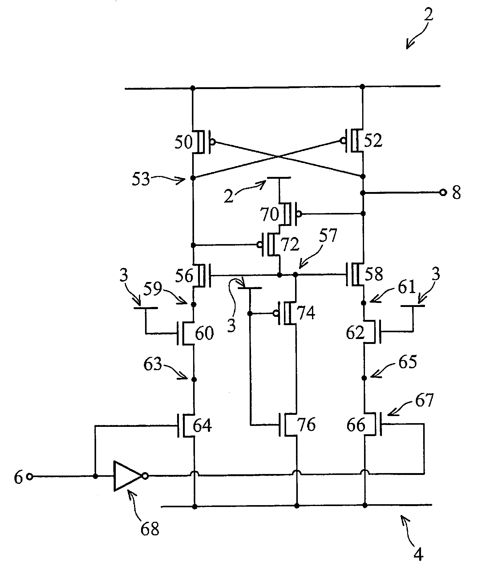
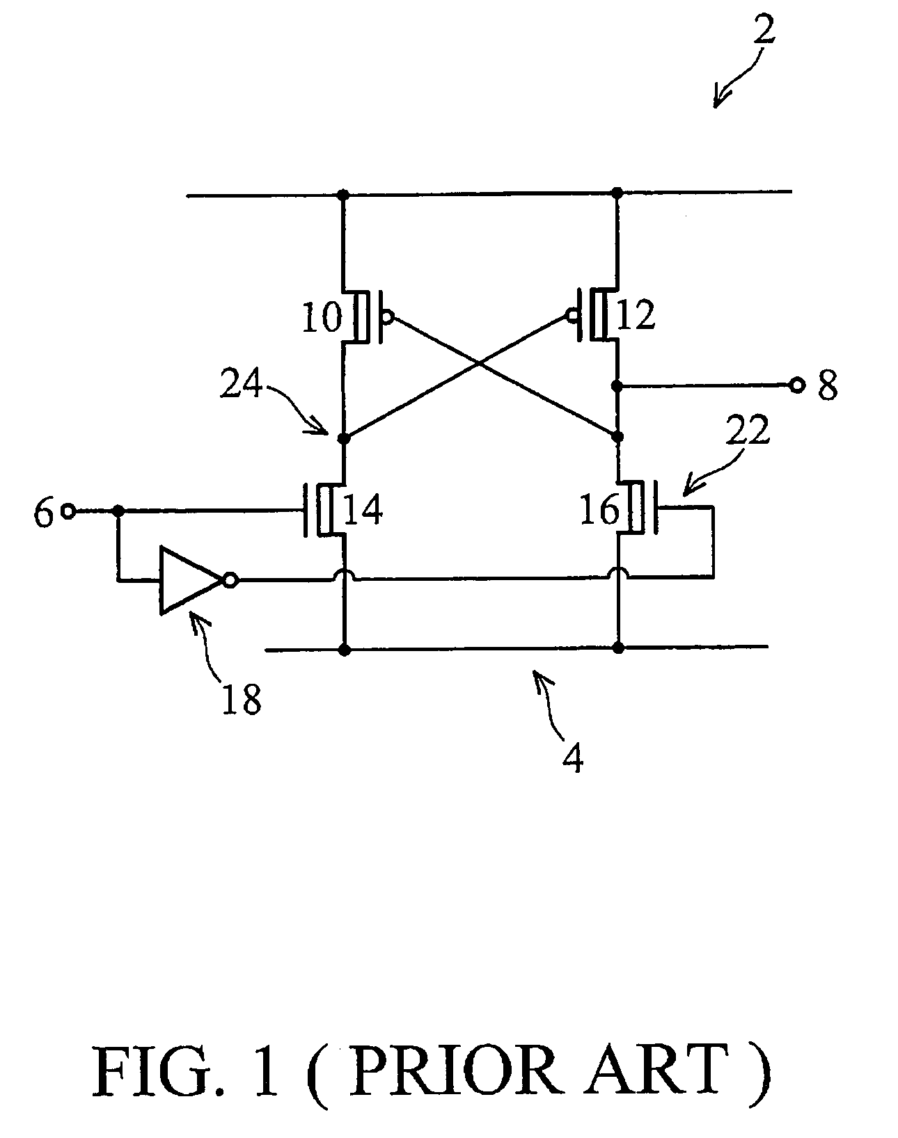
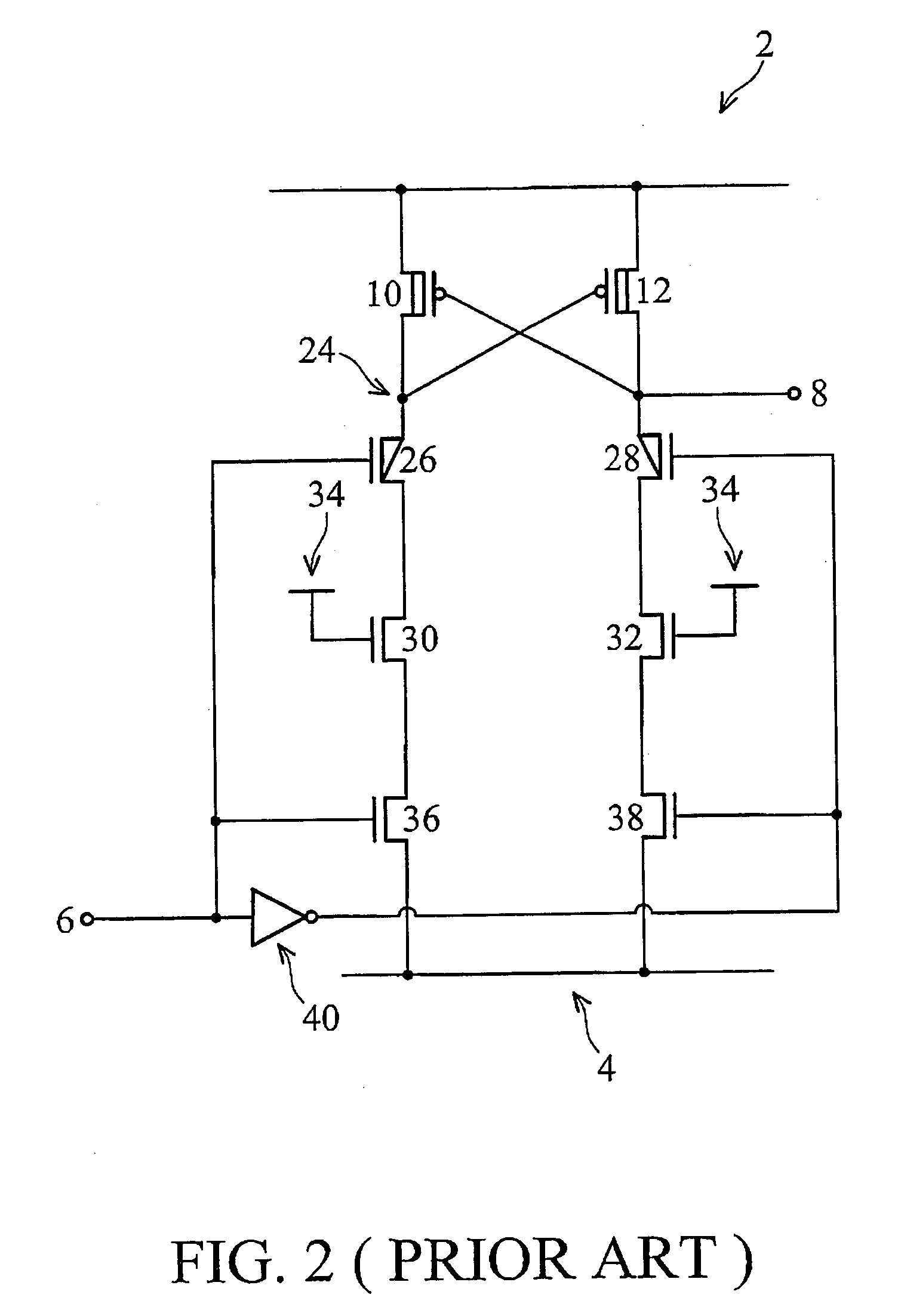
[0022]The preferred embodiments are illustrated in FIGS. 3 through 6 wherein like reference numbers are used to designate like elements throughout the various views and illustrative embodiments of the present invention. The nodes in the circuit illustrated are represented with numerical values.

[0023]FIG. 3 illustrates a schematic view of a preferred embodiment of the present invention. Node 2 is coupled to a high voltage VDDIO, and node 4 is coupled to a VSS, typically the ground potential or 0V. Node 6 is the signal input node and node 8 is the signal output node. The input ...


PUM


Abstract

A boost-biased level shifter is described. In the preferred embodiments of the present invention, a voltage divider circuit divides the high voltage applied on the receiver circuit that receives the input signal, a refresh and self-bias circuit maintains and refreshes a bias voltage that is high enough to turn on the transistors in the voltage divider circuit, and a voltage output circuit outputs a signal having the amplitude of a higher power supply source, which is higher than the input signal amplitude. The preferred embodiments can operate at input signals having a lower amplitude. The performance is improved.

Description

TECHNICAL FIELD[0001]This invention relates generally to digital circuits, and more specifically to digital level shifters.BACKGROUND[0002]A level shifter is a circuit that converts an input signal having the voltage amplitude of VDD1 into an output signal having the voltage amplitude of VDD2. Typically, the amplitude is converted by fixing the lower potential side and converting the potential at the higher potential side. Level shifters are widely used in integrated circuits where more than one type of circuit, each with different operating voltage amplitudes, are integrated together.[0003]A common application for a level shifter is shifting the voltage of a signal transferred between an IO circuit and a core circuit in an integrated circuit device. Traditionally, the IO operating voltage was compatible with the core operating voltage. However, with the shrinking of VLSI circuits, the operating voltage of core circuits has steadily been lowered, while the IO operating voltage has s...

Claims


Application Information

Patent Timeline
Patent Type & Authority Patents(United States)
IPC IPC(8): H03L5/00
CPCH03K3/356113H03K17/102
Inventor CHEN, KER-MIN
Owner TAIWAN SEMICON MFG CO LTD
Why Eureka
Try Eureka