Capacitor for a semiconductor device and method for fabrication therefor

Inactive Publication Date: 2005-01-25
BELL SEMICON LLC
View PDF9 Cites 25 Cited by
  • Summary
  • Abstract
  • Description
  • Claims
  • Application Information

AI Technical Summary

Benefits of technology

The capacitor electrodes and insulator are preferably deposited within the trench, lining the trench sidewalls and bottom. In this manner, a recess is formed over the second capacitor electrode in which a conductive metal is deposited forming a metal lead to connect the capacitor to another device component. The metal lead preferably consists of copper or a copper alloy deposited within the recess. The films and conductive metal are then planarized forming a planar top surface of the capacitor that is substantially coplanar with a top surface

Problems solved by technology

In addition, the chemical mechanical polishing of copper may compromise the capacitors rel

Method used


Image

  • Capacitor for a semiconductor device and method for fabrication therefor
  • Capacitor for a semiconductor device and method for fabrication therefor
  • Capacitor for a semiconductor device and method for fabrication therefor

Examples


Example

DETAILED DESCRIPTION OF THE DRAWINGS

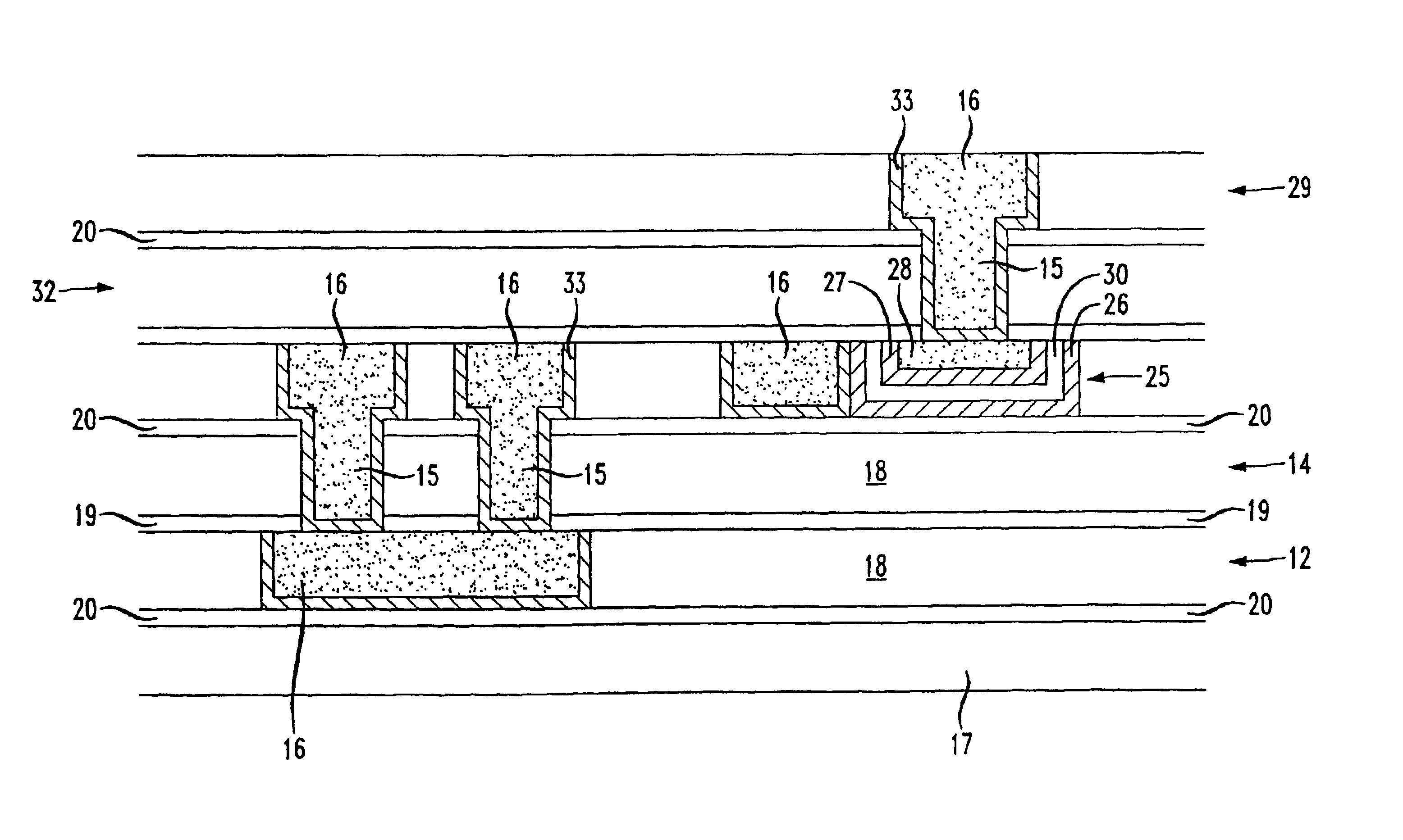
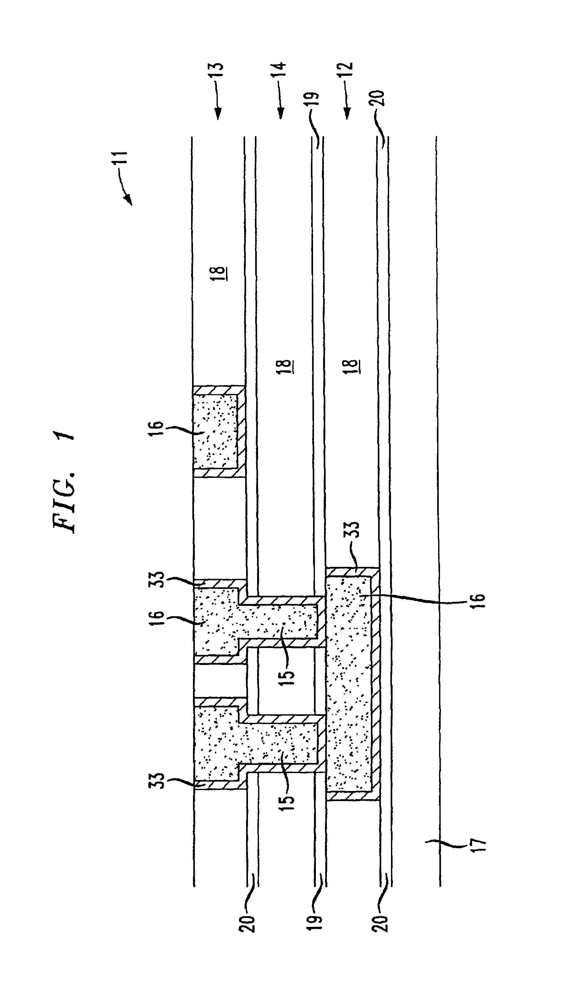
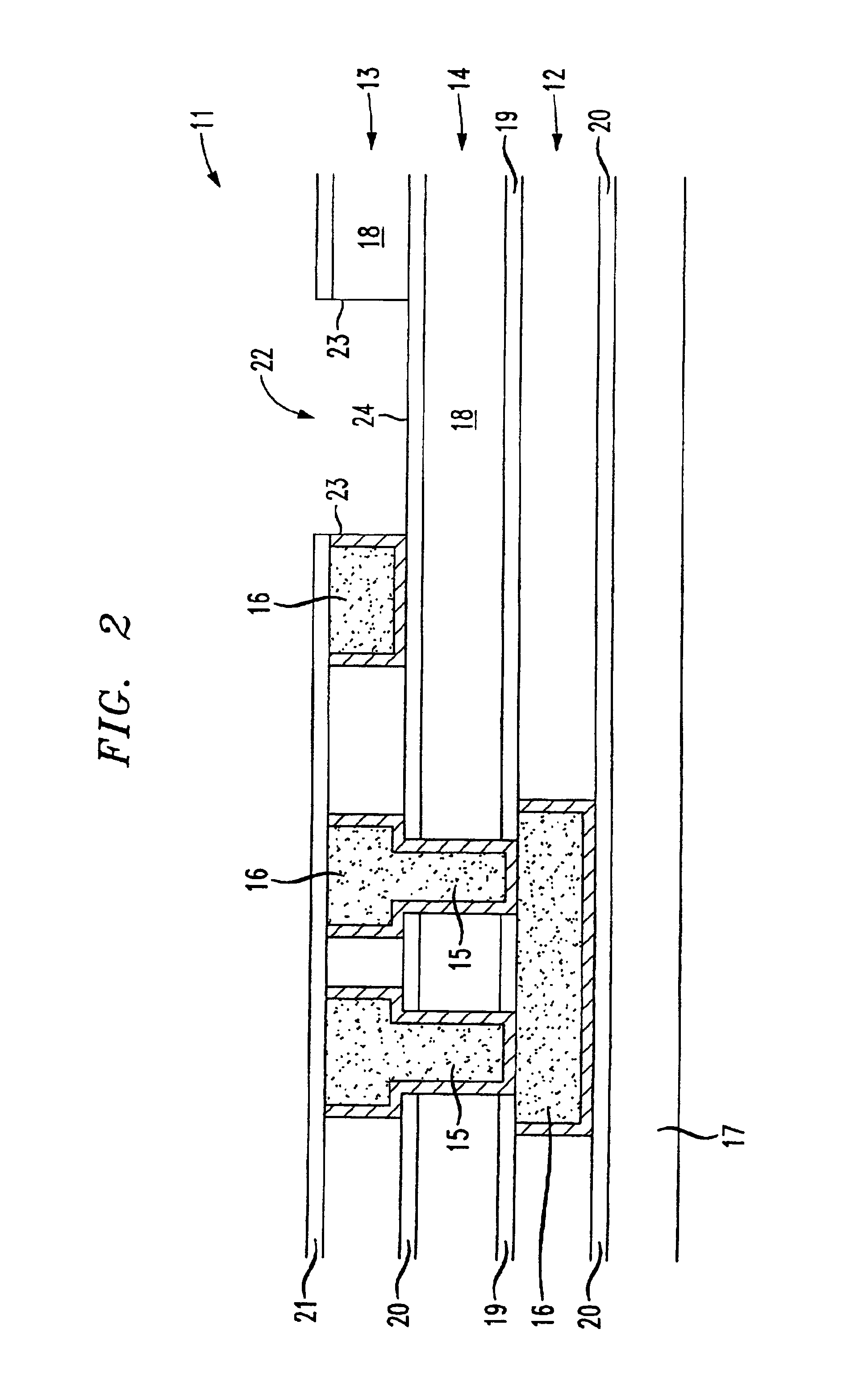
With respect to FIG. 1, an interconnect structure 11 is shown fabricated on a semiconductor wafer or substrate 17. The term wafer or substrate as used in this specification is understood to include structures formed thereon such as transistors, capacitors, tungsten plugs and contact levels, or other active areas on the substrate 17. The interconnect structure includes a lower metallization layer 12, an upper metallization layer 13 and an insulating layer 14 (also referred to as a “dielectric layer”) disposed between the upper metallization layer 13 and the lower metallization layer 12. For purposes of this description, the term “metallization layer” refers to the structural layer of a semiconductor integrated circuit within which metal conductors and semiconductors are formed. Metallization layers are alternately deposited, during integrated circuit fabrication, with insulating dielectric layers.

The interconnect structure 11 is typically fabricate...


PUM


Abstract

A semiconductor device having a capacitor integrated in a damascene structure. In one embodiment, the capacitor is formed entirely within a metallization layer of a damascene structure, having therein a semiconductor device component. Preferably, the capacitor is formed within a trench, having been etched in the dielectric material of the metal layer and the capacitor includes a first capacitor electrode formed within the recess in electrical contact with the device component of the metallization layer. An insulator may be formed over the first capacitor electrode, with a second capacitor electrode formed over the insulator. These elements are preferably conformally deposited within the trench, thereby forming a recess, a portion of which extends within the trench. A subsequently fabricated device component may then be placed in electrical contact with the second capacitor electrode.

Description

BACKGROUND OF THE INVENTIONThe present invention relates in general to fabricating semiconductor devices, and, more specifically, to the integration of capacitors in damascene interconnect structures.Capacitors are used extensively in electronic devices for storage of electric charge. The capacitors essentially comprise two conductive plates separated by an insulator. The capacitance, or amount of charge held by the capacitor per applied voltage, depends upon the area of the plates, the distance between the plates, and the dielectric values of the insulator. Capacitors are used in filters, analog to digital converters, digital memory devices, and various control applications.Metal-based capacitors are typically incorporated into a device using a subtractive metal etch process, which is conventionally used to form aluminum lines. However, copper has increased in popularity as a metal of choice for fabrication of metallization layers. Copper has a lower resistivity, which allows for t...

Claims


Application Information

Patent Timeline
IPC IPC(8): H01L21/02H01L23/522H01L21/70H01L23/532H01L21/768H01L23/52H01L21/3205H01L21/822H01L27/04H01L27/108
CPCH01L21/76838H01L23/5223H01L28/60H01L28/40H01L23/53228H01L2924/0002H01L2924/00H10B12/00
Inventor THOMAS, SYLVIA W.PARRISH, MICHAEL JAYIVANOV, TONY G.HARRIS, EDWARD BELDENGREGOR, RICHARD WILLIAMCARROLL, MICHAEL SCOTT
Owner BELL SEMICON LLC
Why Eureka
Try Eureka