

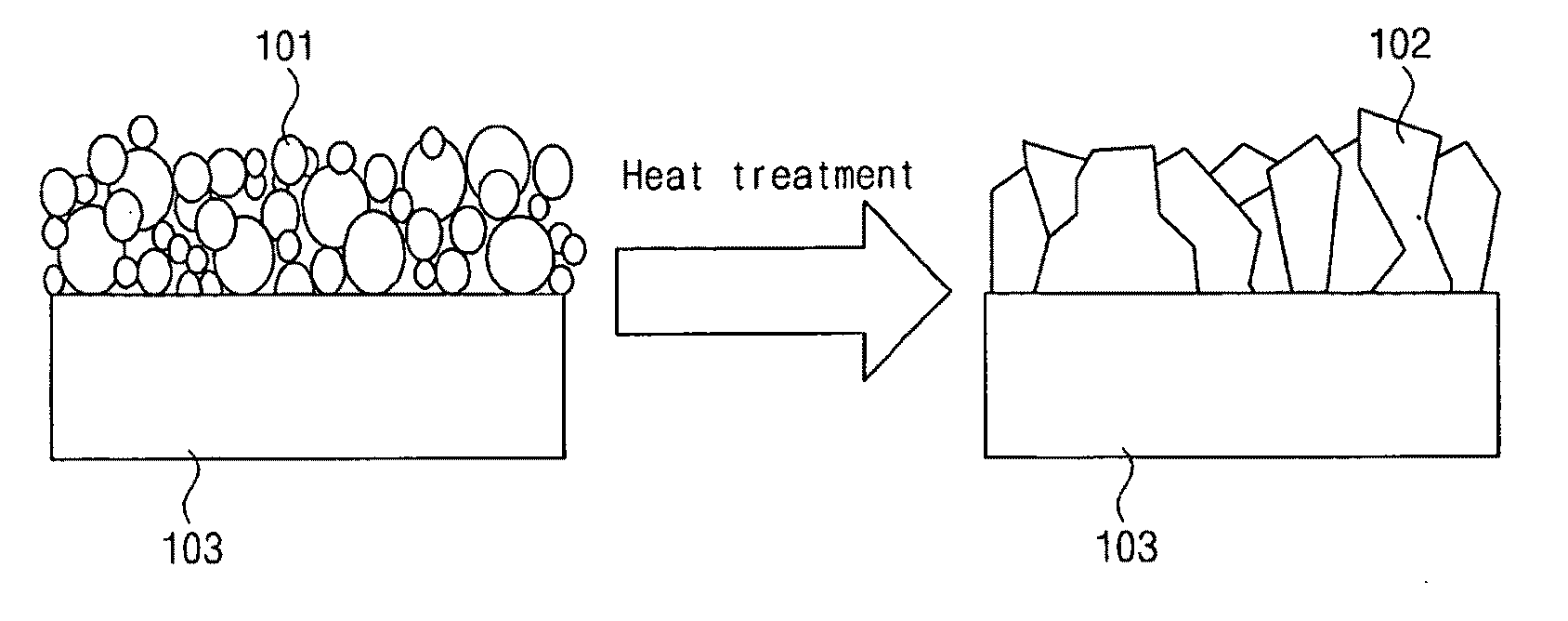
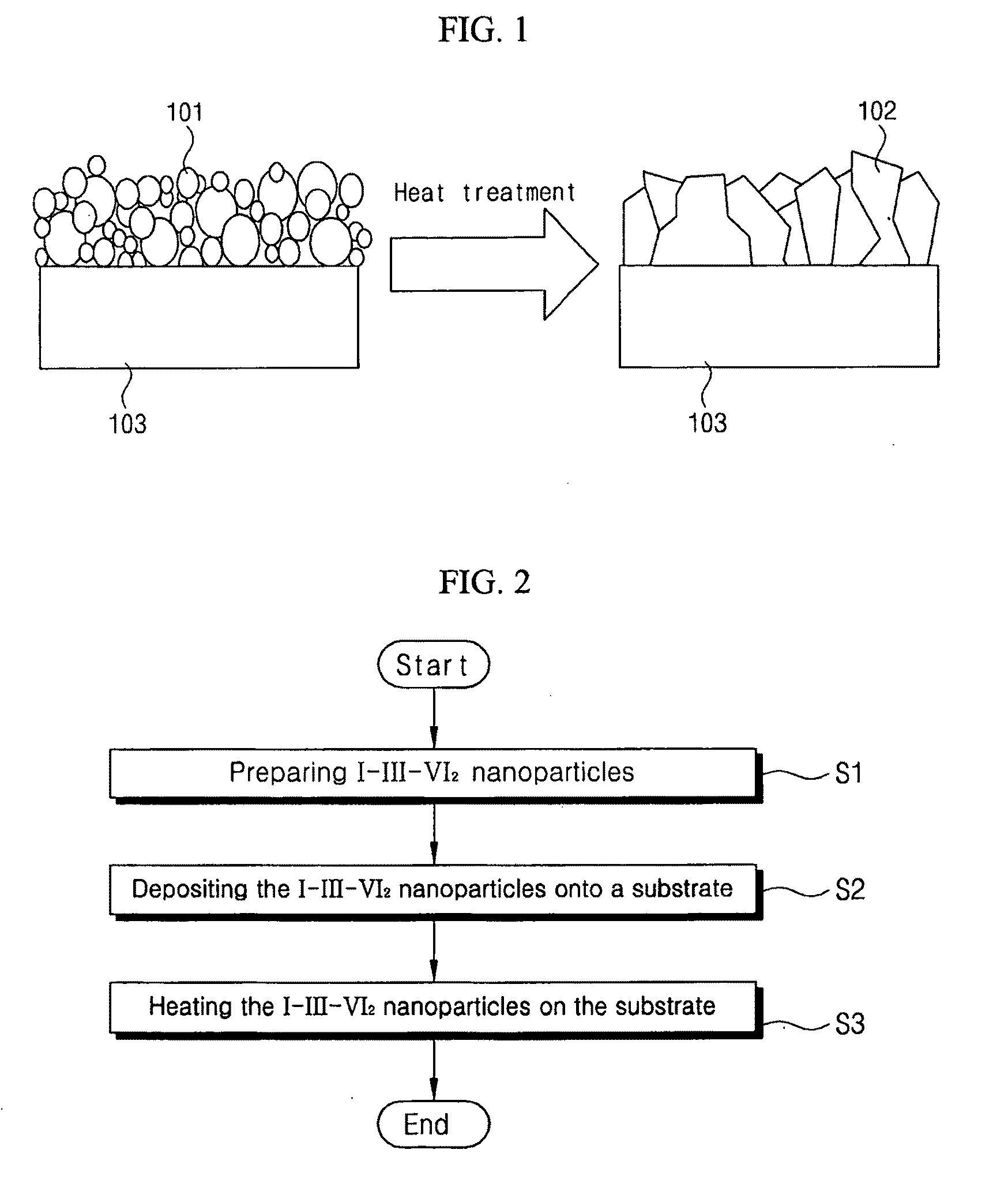
Synthesis of i-iii-vi2 nanoparticles and fabrication of polycrystalline absorber layers
- Summary
- Abstract
- Description
- Claims
- Application Information
AI Technical Summary
Benefits of technology
Problems solved by technology
Method used
Image

Examples
example 1
Preparation of CuInSe2 Nano Particles
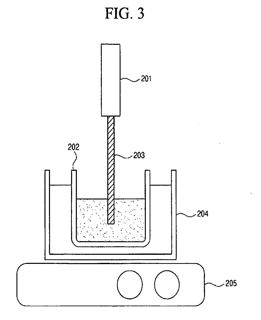
[0053]Cu(CH3COO)2, In(CH3COO)3 and Se powders were placed into a reactor (102) with the molar ratio of 1:1:2. The reactor was charged with triethylene tetramine, 1-butyl-3-methylimidazolinium trifluoromethanesulfonate and an alcoholic solvent. The mixture was subjected to ultrasonication for 4 hours at 100° C. and then allowed to cool in the air. The resulted product was centrifuged to remove the solvent, washed several times with distilled water and ethanol, and then dried for 4 hours at 80° C. under the atmospheric pressure.
[0054]For qualitative analysis to find out the composition of thus obtained CuInSe2 nanoparticles as well as their particle size distribution, EDS (Energy Dispersive Spectroscopy) and Scanning Electron Microscopy (SEM) were carried out, and the results thereof were disclosed in FIGS. 4 and 5. It was found that the final product had the ratio of each element of Cu:In:Se being 0.96:1.00:2.04 and was comprised of particles havi...
example 2
First Reuse of Solvent
[0055]By reusing the separated solvent by centrifugation in Example 1, CuInSe2 nanoparticles were synthesized. First, Cu(CH3COO)2, In(CH3COO)3 and Se powders were placed into a reactor with the molar ratio of 1:1:2. The reactor was charged with the solvent obtained from Example 1. The mixture was subjected to ultrasonication and then dried in the air. The resulted product was centrifuged to remove the solvent, washed several times with distilled water and an alcohol, and dried for 4 hours at 80° C. under the atmospheric pressure. The obtained nanoparticles were subjected to powder X-ray diffraction, and the graph showing the results was illustrated in FIG. 7(a).
example 3
Second Reuse of Solvent
[0056]By reusing the separated solvent by centrifugation in Example 2, CuInSe2 nanoparticles were synthesized. Materials for Cu, In and Se were placed into a reactor. The reactor was charged with the solvent obtained from Example 3. To the resulted solution, ultrasonic waves were applied. From this point, for the subsequent steps, the same steps as in Example 2 were used to prepare nanoparticles. The graph of powder X-ray diffraction analysis of the obtained nanoparticles was illustrated in FIG. 7(b).
PUM
| Property | Measurement | Unit |
|---|---|---|
| Temperature | aaaaa | aaaaa |
Abstract
Description
Claims
Application Information