Supercharge Your Innovation With Domain-Expert AI Agents!

Packaged semiconductor device for radio frequency shielding

a technology of radio frequency shielding and semiconductor devices, applied in semiconductor devices, semiconductor/solid-state device details, substation/switching arrangement details, etc., can solve the problems of high cost, high complexity, and small size, and achieve the effect of reducing the cost of traditional faraday shields

Inactive Publication Date: 2005-01-25
SILICON BANDWIDTH
View PDF32 Cites 15 Cited by
  • Summary
  • Abstract
  • Description
  • Claims
  • Application Information

AI Technical Summary

Benefits of technology

"The present invention provides a semiconductor package that can be prefabricated and electrically shields a semiconductor chip. It includes a conductive strip with a top rail, bottom rail, connecting member, and conductive contacts. The conductive contacts extend from the connecting member and can be insert molded or sandwiched in a housing. The package also includes a radio frequency shield and an internal cavity for a second semiconductor device. The invention also provides a method of fabricating the semiconductor package and a conductive cover for it. The technical effects of the invention include improved electrical shielding, reduced assembly limitations, and improved reliability and performance of semiconductor devices."

Problems solved by technology

Furthermore, premiums are often placed on small size, complexity, and high performance.
Thus, such high-speed digital systems can radiate energy (noise) that interferes with sensitive analog circuits.
While faraday shielding has been widely used to protect sensitive analog circuits from interference, the traditional faraday shields tend to be expensive.
Moreover, the traditional faraday shield is not particularly flexible.
While prior art semiconductor packages have been successful, they are not without problems.
First, as semiconductor devices are mounted closer and closer together, the problem of cross-talk increases.
This is a significant problem with analog circuits that have high impedance levels since they are particularly sensitive to crosstalk.
Prior art semiconductor packages usually do not provide electrical and electromagnetic isolation of their components.
Furthermore, prior art semiconductor packages can be inconvenient and expensive because they require semiconductor manufacturers to not only have semiconductor fabrication equipment on site, but also both wire bonding and encapsulation equipment.

Method used


Image

  • Packaged semiconductor device for radio frequency shielding
  • Packaged semiconductor device for radio frequency shielding
  • Packaged semiconductor device for radio frequency shielding

Examples


Embodiment Construction

The principles of the present invention are incorporated in an illustrated semiconductor device. It will be appreciated that while the illustrated semiconductor device displays enhanced properties, others who are skilled in the applicable arts will recognize numerous alternatives and variations. Therefore, the present invention is intended to extend to all alternatives and variations that come under the broad terms of the claims that follow.

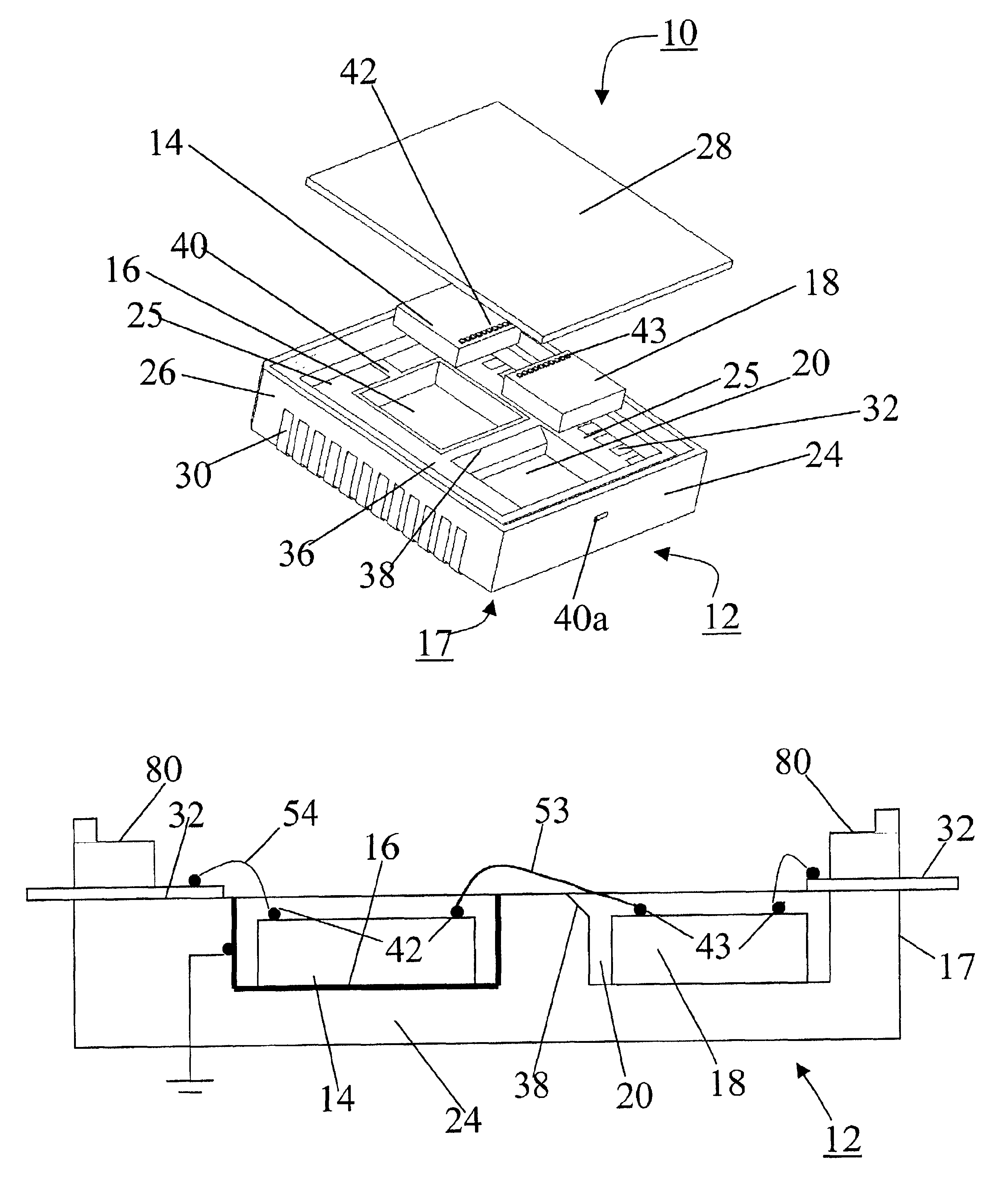
FIG. 2A is an exploded view of a packaged semiconductor device 10 that includes mixed signal integrated circuits in a semiconductor package 12. An IC device such as a high-frequency RF analog integrated circuit 14 mounts in an RF shield 16 that preferably takes the form of a cavity or an open box, for example. A high-speed digital integrated circuit 18 mounts in a cavity 20. The semiconductor package 12 includes a generally rectangular shaped housing 17. Beneficially, housing 17 is a single molded piece having insert molded leads (see below) and ...


PUM


Abstract

A packaged semiconductor device that is fabricated with a plurality of conductive leads defined in a strip that beneficially includes a radio frequency shield box. The conductive contacts are located in a housing, beneficially by insert molding or by sandwiching between a bottom piece and a top piece. The housing can further include a cavity that receives a semiconductor device, and the radio frequency shield can receive another semiconductor device. Bonding conductors electrically connect at least one semiconductor device to another semiconductor device and / or to the conductive contacts. A conductive cover is disposed over the housing. The cavity beneficially includes a beveled wall and the conductive leads and the radio frequency shield are beneficially comprised of copper.

Description

BACKGROUND OF THE INVENTION1. Field of the InventionThe present invention relates to semiconductor packages. More particularly, the present invention relates to semiconductor packages capable of incorporating radio frequency shielding.2. Discussion of the Related ArtModem electronic devices, for example cellular phones and pagers, require a seamless integration of analog and digital subsystems. Furthermore, premiums are often placed on small size, complexity, and high performance. Thus, sensitive analog circuits frequently need to be placed very close to high-speed digital systems.High-speed digital systems can switch more then one hundred million times a second. At such switching speeds, switching currents tend to be high. Thus, such high-speed digital systems can radiate energy (noise) that interferes with sensitive analog circuits. Interference usually takes the form of signal crosstalk. While faraday shielding has been widely used to protect sensitive analog circuits from interf...

Claims


Application Information

Patent Timeline
Patent Type & Authority Patents(United States)
IPC IPC(8): H01L23/02H01L23/057H01L23/498H01L23/552H01L23/48
CPCH01L23/057H01L23/49861H01L23/552H01L24/32H01L2924/01033H01L24/48H01L2924/3025H01L2924/3011H01L2924/16195H01L2924/1617H01L2924/15165H01L2924/15153H01L2924/14H01L2924/01082H01L2224/32014H01L2224/32245H01L2224/48091H01L2224/48137H01L2224/48247H01L2224/48464H01L2224/48465H01L2224/73265H01L2924/01029H01L2924/00014H01L2924/00H01L2224/05599H01L2224/45099H01L2224/85399H01L2224/45015H01L2924/207
Inventor CRANE, JR., STANFORD W.JEON, MYOUNG-SOOALCARIA, VICENTE D.
Owner SILICON BANDWIDTH
Features
  • R&D
  • Intellectual Property
  • Life Sciences
  • Materials
  • Tech Scout
  • Unparalleled Data Quality
  • Higher Quality Content
  • 60% Fewer Hallucinations
Learn More