Variable delay circuit and method, and delay locked loop, memory device and computer system using same

a delay circuit and delay lock technology, applied in the field of clock circuits, can solve the problems of significant disadvantage of inverting the clock signal, additional delay can be a significant problem, and the extra circuitry and consequent cost of these additional inverters can be significan

Inactive Publication Date: 2005-02-01
ROUND ROCK RES LLC
View PDF48 Cites 41 Cited by
  • Summary
  • Abstract
  • Description
  • Claims
  • Application Information

AI Technical Summary

Benefits of technology

A variable delay circuit produces a delayed clock signal from an input clock signal by coupling the input clock signal through a plurality of inverting logic circuits arranged in series with each other. A delay select circuit, such as a shift register, receives at least one delay command signal indicative of a delay of the variable delay circuit. The delay select circuit then generates at least one control signal responsive to the delay command signal. The variable delay circuit also includes a clock transfer control circuit coupled to the inverting logic circuits and the delay select circuit. The clock transfer control circuit receives the input clock signal and adjusts the delay of the delayed clock signal responsive to the at least one control signal. The delay is adjusted by varying the number of inverting logic circuits through which the input clock signal is coupled between the clock input terminal and the clock output terminal. The clock transfer control circuit also adjusts the polarity of the input clock signal between the clock input terminal and the clock output terminal as a function of the at least one control signal so that the correct polarity of the delayed clock signal is maintained despite being coupled through a variable number of inverting logic circuits.

Problems solved by technology

Although the variable delay circuit 10 of FIG. 1 provides adequate performance under some circumstances, it has the significant disadvantage of inverting the clock signal as the delay is switched from one inverter 12a,b,c,e,d,e to the next.
This additional delay can be a significant problem in some applications.
The extra circuitry and consequent expense of these additional inverters can be significant, particularly where a large number of inverters are need to provide a large delay or a large number of delay increments.

Method used


Image

  • Variable delay circuit and method, and delay locked loop, memory device and computer system using same
  • Variable delay circuit and method, and delay locked loop, memory device and computer system using same
  • Variable delay circuit and method, and delay locked loop, memory device and computer system using same

Examples


Embodiment Construction

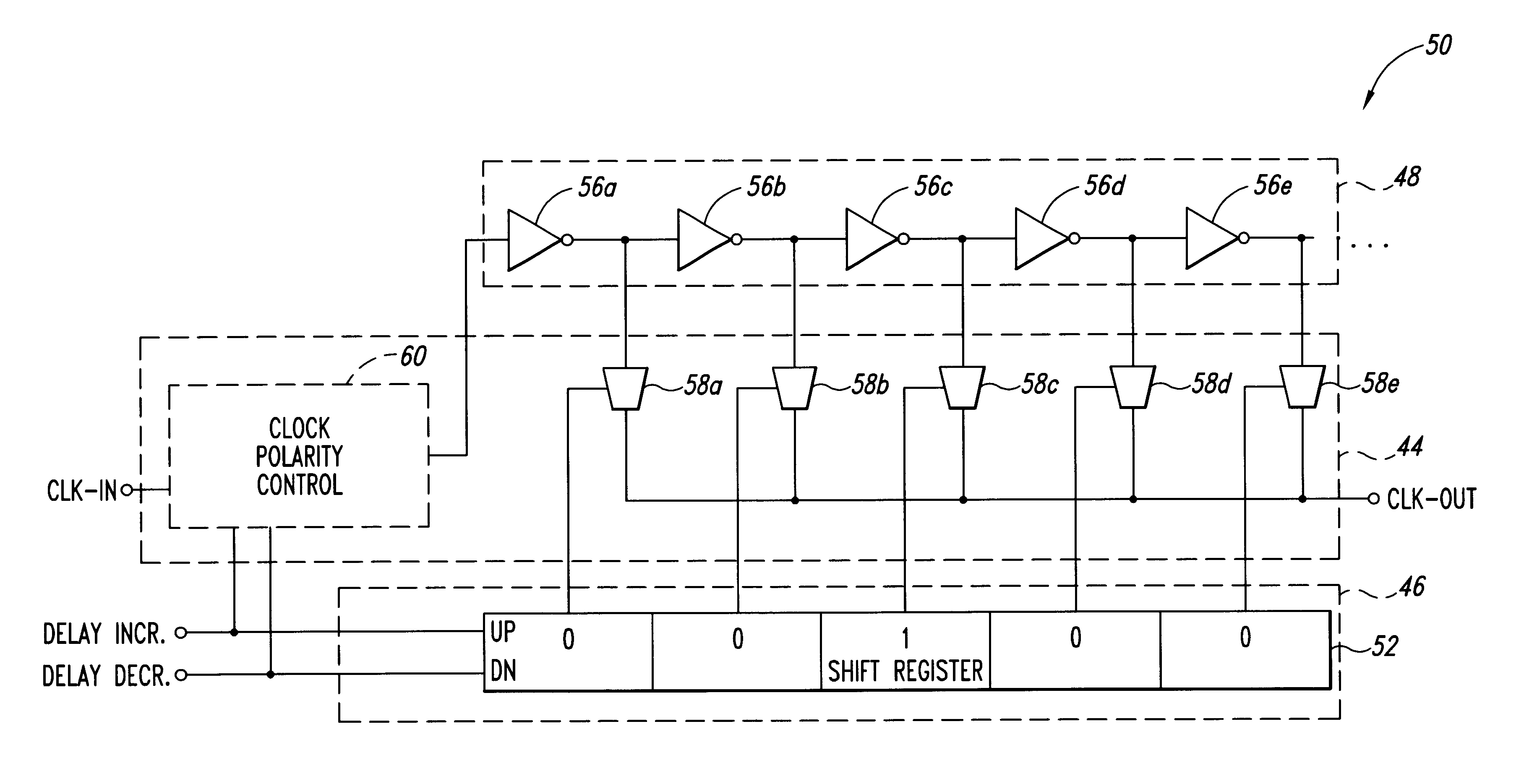
FIG. 3 is a block diagram of one embodiment of a variable delay circuit 40 according to the present invention. The delay circuit 40 included a clock transfer control circuit 44 to which an incoming clock signal CLK-IN is applied and from which a delayed clock signal CLK-OUT is generated. The transfer control circuit 44 also receives DELAY INCR and DELAY DECR pulses that are also applied to a delay select circuit 46. The clock transfer circuit 44 is coupled to the delay select circuit 46 and to a plurality of inverting logic circuits 48a,b,c,d.

In operation, the delay select circuit 46 outputs a signal on one of its interconnections to the clock transfer circuit 44 that selects the magnitude of the delay of the CLK-OUT signal. The interconnection on which the select signal is generated is shifted in one direction to increase the delay responsive to each DELAY INCR pulse, and is shifted in the other direction to decrease the delay responsive to each DELAY DECR pulse. The select signal...


PUM


Abstract

A variable delay circuit uses a plurality of inverters or inverting gates as delay elements in a delay line. In one embodiment of the invention, the point in the delay circuit at which an input clock signal enters the delay circuit is adjusted to vary the delay of an output clock signal. In another embodiment, the point in the delay circuit from which the output clock signal exits the delay circuit is adjusted to vary the delay of an output clock signal. In either case, the polarity of the input or output clock signal is adjusted as the delay is adjusted so there are always an even number of inverters or inverting gates between an input terminal to which the input clock signal is applied and an output terminal from which the output clock signal is generated.

Description

TECHNICAL FIELDThe invention relates clock circuits, and, more particularly, to a circuit and method for providing a clock signal with a variable delay in a manner that uses relatively little circuitry.BACKGROUND OF THE INVENTIONVariable delay circuits for delaying digital signals are in common use in a wide variety of integrated circuit devices. For example, variable delay circuits are commonly used as part of delay locked loops in integrated circuit memory devices. An example of a conventional variable delay circuit 10 is shown in FIG. 1. The variable delay circuit 11 includes a series of inverters 12a,b,c,d,e, the first of which 12a receives a clock signal CLK. The output of each inverter 12a,b,c,e,d,e is coupled to a respective pass gate 16a,b,c,e,d,e that are selectively enabled by respective stages of a shift register 18. Only one of the stages of the. shift register stores a logic “1”, and all of the other stages store a logic “0”. The pass gate 16a,b,c,e,d,e that receives th...

Claims


Application Information

Patent Timeline
Patent Type & Authority Patents(United States)
IPC IPC(8): G11C7/00G11C7/22H03L7/089H03L7/081H03L7/08
CPCG11C7/22H03L7/089H03L7/0814G11C7/222
Inventor GOMM, TYLER J.
Owner ROUND ROCK RES LLC
Why Eureka
Try Eureka