Analog-to-digital conversion method and device

a conversion method and digital data technology, applied in analogue/digital conversion, physical parameter compensation/prevention, instruments, etc., can solve the problems of reducing the number of bits constituting digital data produced, reducing resolution, and limited resolution improvement in analog-to-digital conversion, so as to improve resolution and the effect of variable driving voltag

Inactive Publication Date: 2005-02-01
DENSO CORP
View PDF15 Cites 41 Cited by
  • Summary
  • Abstract
  • Description
  • Claims
  • Application Information

AI Technical Summary

Benefits of technology

In the analog-to-digital conversion device having the twenty-fourth aspect of the present invention implemented therein, as mentioned above, an output of each of the delay units constituting the second pulse delay circuit is not needed to actuate any other circuit. A driving voltage to be applied to each of the delay units constituting the second pulse delay circuit may be lower than that to be applied to each of the delay units constituting the first pulse delay circuit. Moreover, the variance of the driving voltage may be larger. According to the present invention, the amplification factors n and m at which the amplification circuits amplify the input voltage and the offset voltages to be added by the voltage shift circuits are determined based on their properties. This leads to an improved resolution in the analog-to-digital conversion performed by the analog-to-digital conversion device.

Problems solved by technology

This poses a problem in that improvement of the resolution in analog-to-digital conversion is limited by the gate circuit manufacturing technology.
However, shortening the sampling cycle TS leads to a decrease in the number of bits constituting digital data produced in proportion to the input voltage Vin, and eventually to a reduction in a resolution.
Therefore, the analog-to-digital conversion devices cannot be adapted to an application requiring high-speed analog-to-digital conversion that yields a desired resolution (for example, 10 bits and 1 MHz) because of the insufficient conversion rate.
It therefore takes too much time to work out a desired digitized value.
This poses a problem in that the configuration of the A / D conversion device becomes complex and the cost thereof increases.

Method used


Image

  • Analog-to-digital conversion method and device
  • Analog-to-digital conversion method and device
  • Analog-to-digital conversion method and device

Examples


first embodiment

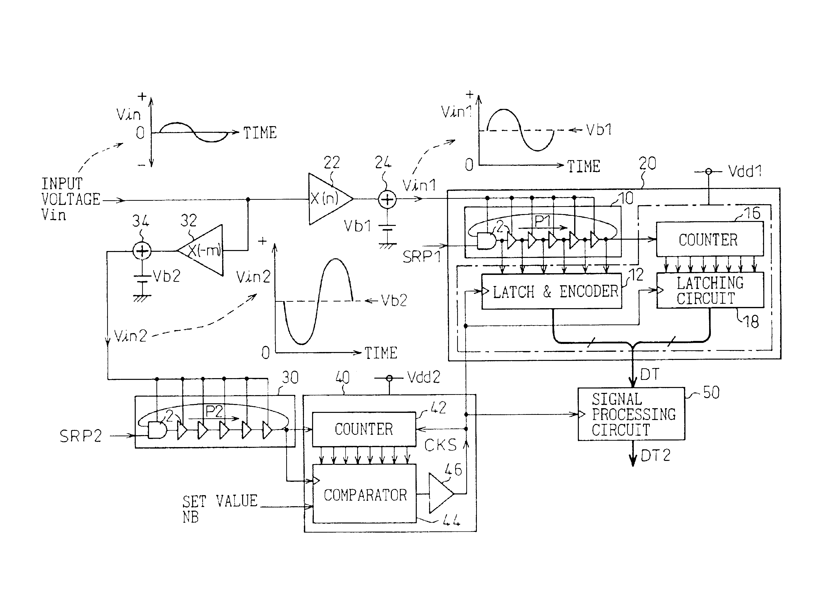
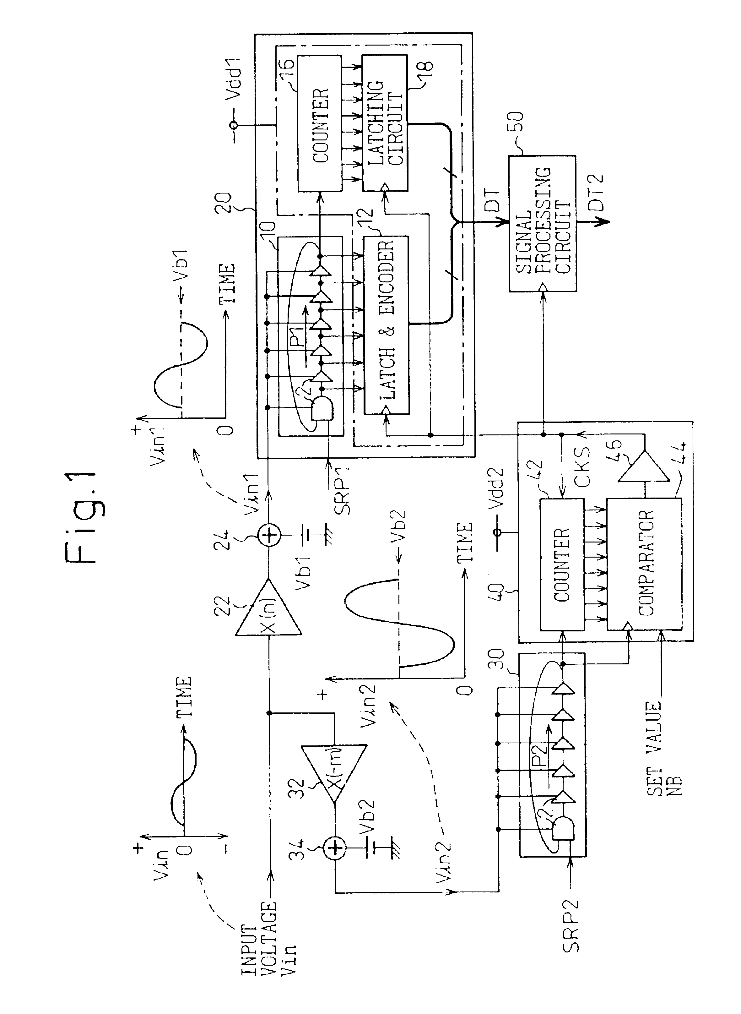
FIG. 1 shows the overall configuration of an analog-to-digital conversion device of the first embodiment in which the present invention is implemented.

The analog-to-digital conversion device of the present embodiment is a device for converting an input voltage Vin into numerical data according to the analog-to-digital conversion method having the first aspect of the present embodiment implemented therein. Herein, the analog-to-digital conversion device is designed in efforts to accomplish the first object of the present invention (that is, to improve the resolution in analog-to-digital conversion or raise an analog-to-digital conversion rate). Similarly to the conventional analog-to-digital conversion device shown in FIG. 8B, the analog-to-digital conversion device includes an analog-to-digital conversion unit 20 composed of a pulse delay circuit 10 realized with a ring delay line (RDL), a latch and encoder 12, a counter 16, and a latching circuit 18. The pulse delay circuit 10 is e...


PUM


Abstract

An analog-to-digital conversion device is provided that uses pulse delay circuits to convert an input voltage into numerical data and offers a high resolution in analog-to-digital conversion or a high analog-to-digital conversion rate. The analog-to-digital conversion device includes an analog-to-digital conversion unit having a pulse delay circuit composed of a plurality of delay units. The delay units are driven with a voltage produced by amplifying or shifting an input voltage. The number of delay units through which a pulse signal has passed during a predetermined sampling cycle is adopted as a digitized value of the input voltage. Herein, delay units constituting another pulse delay circuit are driven with a voltage produced by inversely amplifying or shifting the input voltage. Every time the number of delay units through which a pulse signal has passed within the pulse delay circuit reaches a predetermined value determined with a set value, a sampling signal is transferred to the analog-to-digital conversion unit.

Description

BACKGROUND OF THE INVENTION1. Field of the InventionThe present invention relates to an analog-to-digital conversion method and device for converting an input voltage into numerical data.2. Description of the Related ArtIn the past, analog-to-digital (A / D) conversion devices have been used to convert an input voltage into numerical data by utilizing a pulse delay circuit that has a plurality of delay units, each of which is realized with a gate circuit, connected in tandem. One analog-to-digital conversion device is disclosed in, for example, Japanese Unexamined Patent Publication Application No. 5-259907.This type of analog-to-digital conversion device is configured as shown in, for example, FIG. 8A or FIG. 8B.To begin with, the analog-to-digital conversion device shown in FIG. 8A has a pulse delay circuit 10 and a latch and encoder 12. The pulse delay circuit 10 has a plurality of delay units 2 connected in tandem. The delay unit 2 delays an input pulse Pin by a predetermined dela...

Claims


Application Information

Patent Timeline
Patent Type & Authority Patents(United States)
IPC IPC(8): H03M1/06H03M1/60H03M1/14H03M1/50
CPCG04F10/005H03M1/0619H03M1/60H03M1/502H03M1/14
Inventor WATANABE, TAKAMOTO
Owner DENSO CORP
Why Eureka
Try Eureka