Nonvolatile semiconductor memory

a semiconductor memory and non-volatile technology, applied in static storage, digital storage, instruments, etc., can solve the problems of increasing manufacturing costs, narrowing of the gap between memory cells, and dropping inner power voltage of flash memory,

Inactive Publication Date: 2005-02-01
KIOXIA CORP
View PDF8 Cites 68 Cited by
  • Summary
  • Abstract
  • Description
  • Claims
  • Application Information

AI Technical Summary

Problems solved by technology

On the other hand, an inner power voltage of the flash memory tends to drop.
With the miniaturization, an interval between the memory cells narrows, and this causes various problems.
This also causes the increase of a manufacturing cost.

Method used


Image

  • Nonvolatile semiconductor memory
  • Nonvolatile semiconductor memory
  • Nonvolatile semiconductor memory

Examples


Embodiment Construction

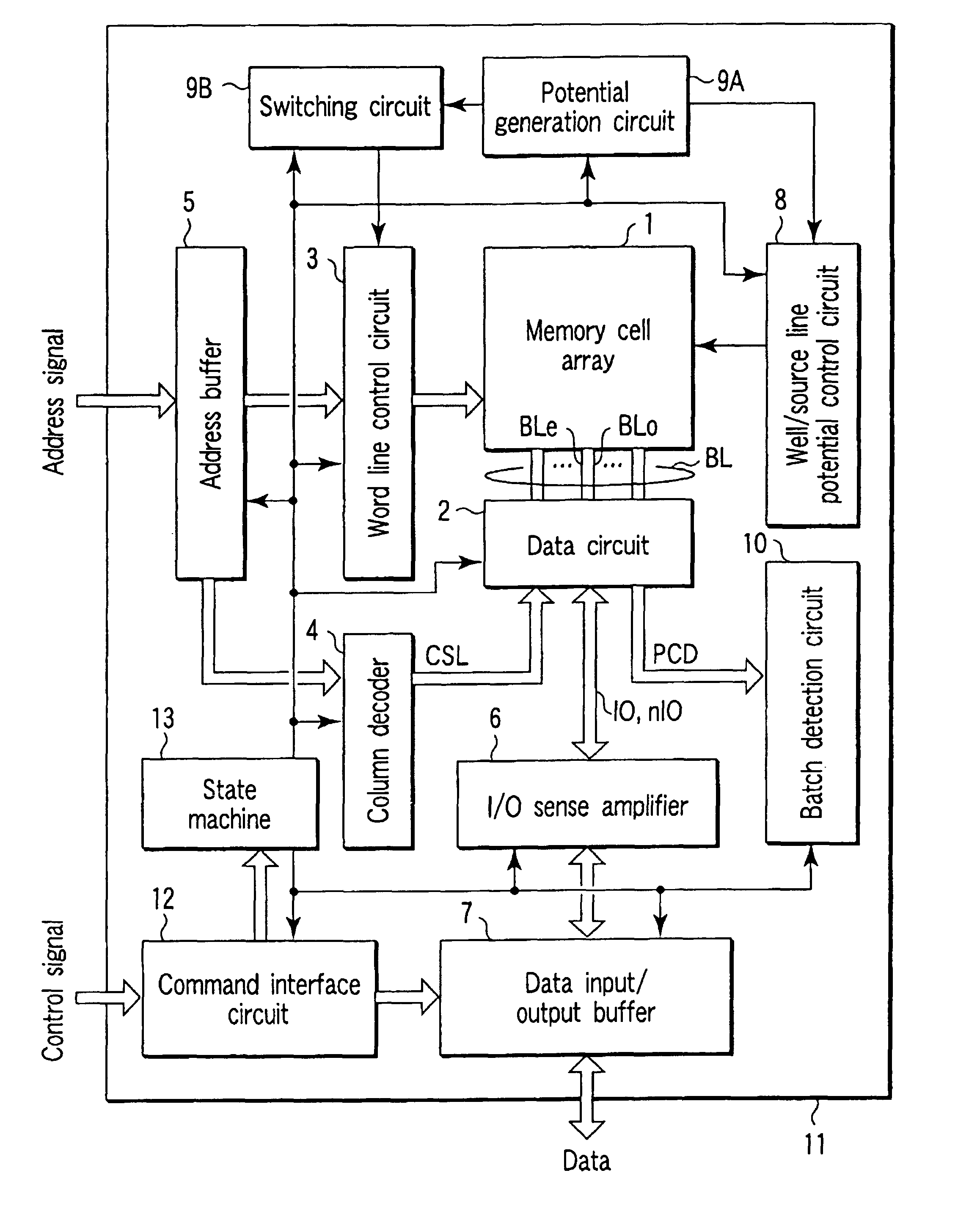
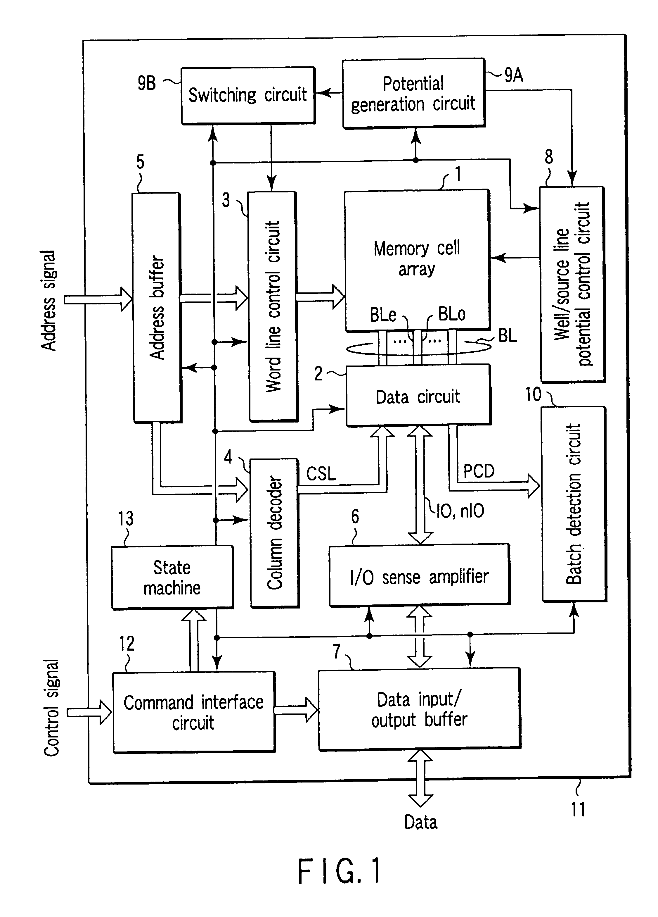
A nonvolatile semiconductor memory according to an embodiment of the present invention will be described hereinafter in detail with reference to the drawings.

1. Assumption

For ease of understanding the following description, prerequisites are defined as follows. Additionally, the prerequisites are set to easily understand the description. The present invention is established even on conditions other than the prerequisites.

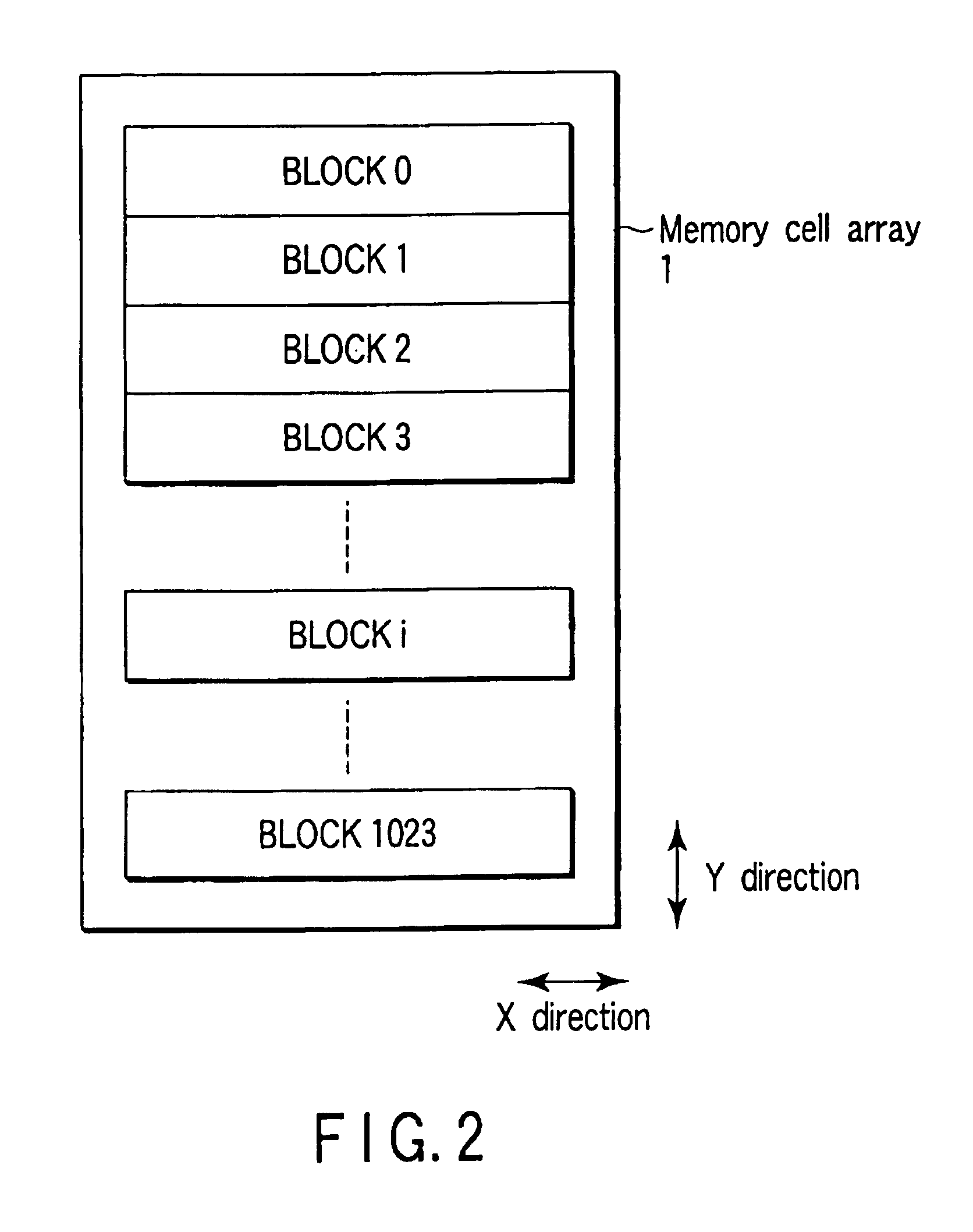
The present invention relates to a multi-level flash memory in which n (n is a natural number of 2 or more) bit data, that is, 2n values are stored in one memory cell. In the following example, a four-level NAND cell type flash memory will be described as a typical example.

It is assumed that four types of data “00”, “01”, “10”, “11” are stored in the memory cell. A state in which a threshold voltage of the memory cell is lowest, for example, a state in which the threshold voltage is negative and belongs to a first threshold value band is assumed as a state in which ...


PUM


Abstract

A bit line is connected to a data circuit for use in a program / read time. The data circuit includes first, second, and third data storage units. The first data storage unit is connected to the bit line. A first data transfer circuit is connected between the first and third data storage units. A second data transfer circuit is connected between the second and third data storage units. The second data storage unit has a function of forcibly changing a value of data of the first data storage unit based on the data stored in the second data storage unit.

Description

CROSS-REFERENCE TO RELATED APPLICATIONSThis application is based upon and claims the benefit of priority from the prior Japanese Patent Application No. 2002-281205, filed Sep. 26, 2002, the entire contents of which are incorporated herein by reference.BACKGROUND OF THE INVENTION1. Field of the InventionThe present invention relates to a nonvolatile semiconductor memory, particularly to a multi-level NAND cell type flash memory such as a four-level NAND cell type flash memory.2. Description of the Related ArtA flash memory is constituted of a memory cell including a floating gate electrode and control gate electrode, and data program / erase is realized by adjustment of a charge amount in the floating gate electrode. The charge amount determines a threshold voltage of the memory cell. For example, a state in which the memory cell has a negative threshold voltage is set to a state “1”, and a state in which the memory cell has a positive threshold voltage is set to a state “0”.In recent ...

Claims


Application Information

Patent Timeline
Patent Type & Authority Patents(United States)
IPC IPC(8): G11C11/56G11C16/02G11C16/04
CPCG11C11/5621G11C11/5628G11C16/0483G11C11/5642G11C11/5635G11C16/04
Inventor TANAKA, TOMOHARU
Owner KIOXIA CORP
Why Eureka
Try Eureka