

Production method for semiconductor chip
- Summary
- Abstract
- Description
- Claims
- Application Information
AI Technical Summary
Benefits of technology
Problems solved by technology
Method used
Image

Examples
Embodiment Construction
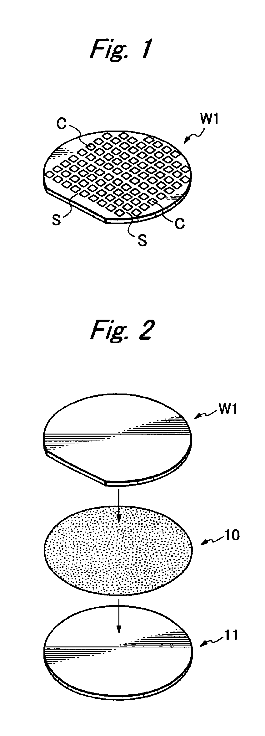
Referring to FIG. 1, a semiconductor wafer W1 has a plurality of chips C defined by crossing streets S on its front side. The semiconductor wafer W1 is divided into squares C individually according to the dividing method of the present invention as follows.
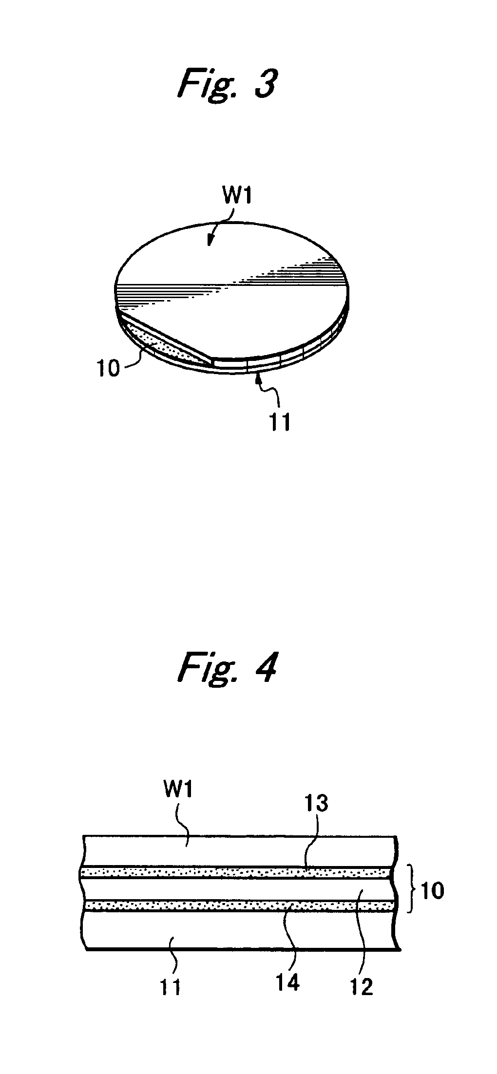
Referring to FIG. 2, the semiconductor wafer W1 is turned upside down, and it is attached to a support disk 11 via an intervening adhesive tape 10, thus providing a wafer-and-support combination (wafer-and-support combining step).
The intervening adhesive tape 10 provides an adhesive layer for sticking the semiconductor wafer W1 to the support disk 11, and the adhesive layer is sensitive to a certain exterior factor for reducing its adhesive force. The adhesive force is caused by the adhesive force and void-less, close attaching force. Adhesive tapes described in JP 63-17981(A) and JP 4-88075(A) may be used.
Referring to FIG. 4, the adhesive tape 10 has its intervening film layer 12 coated on both sides with adhesive agents of diffe...
PUM
 Abstract
Description
Claims
Application Information