Method for manufacturing electronic device and electronic device manufactured thereby
- Summary
- Abstract
- Description
- Claims
- Application Information
AI Technical Summary
Benefits of technology
Problems solved by technology
Method used
Image
Examples
embodiment 1
1. Method for Manufacturing Electronic Device
[0052]As for a method for manufacturing an electronic device according to an embodiment 1 of the present disclosure, a method for manufacturing an active matrix type organic EL display device will be described by way of example.
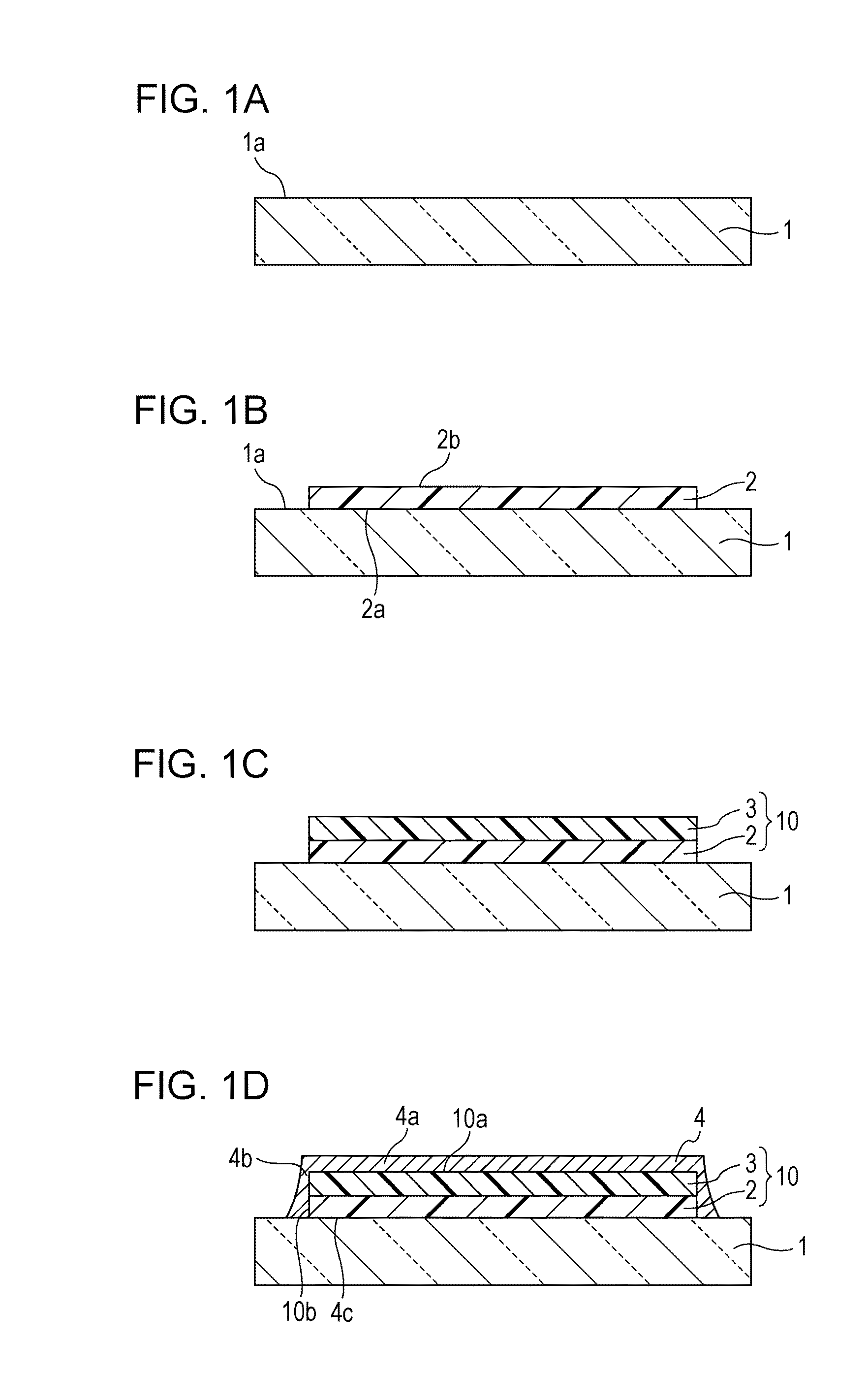
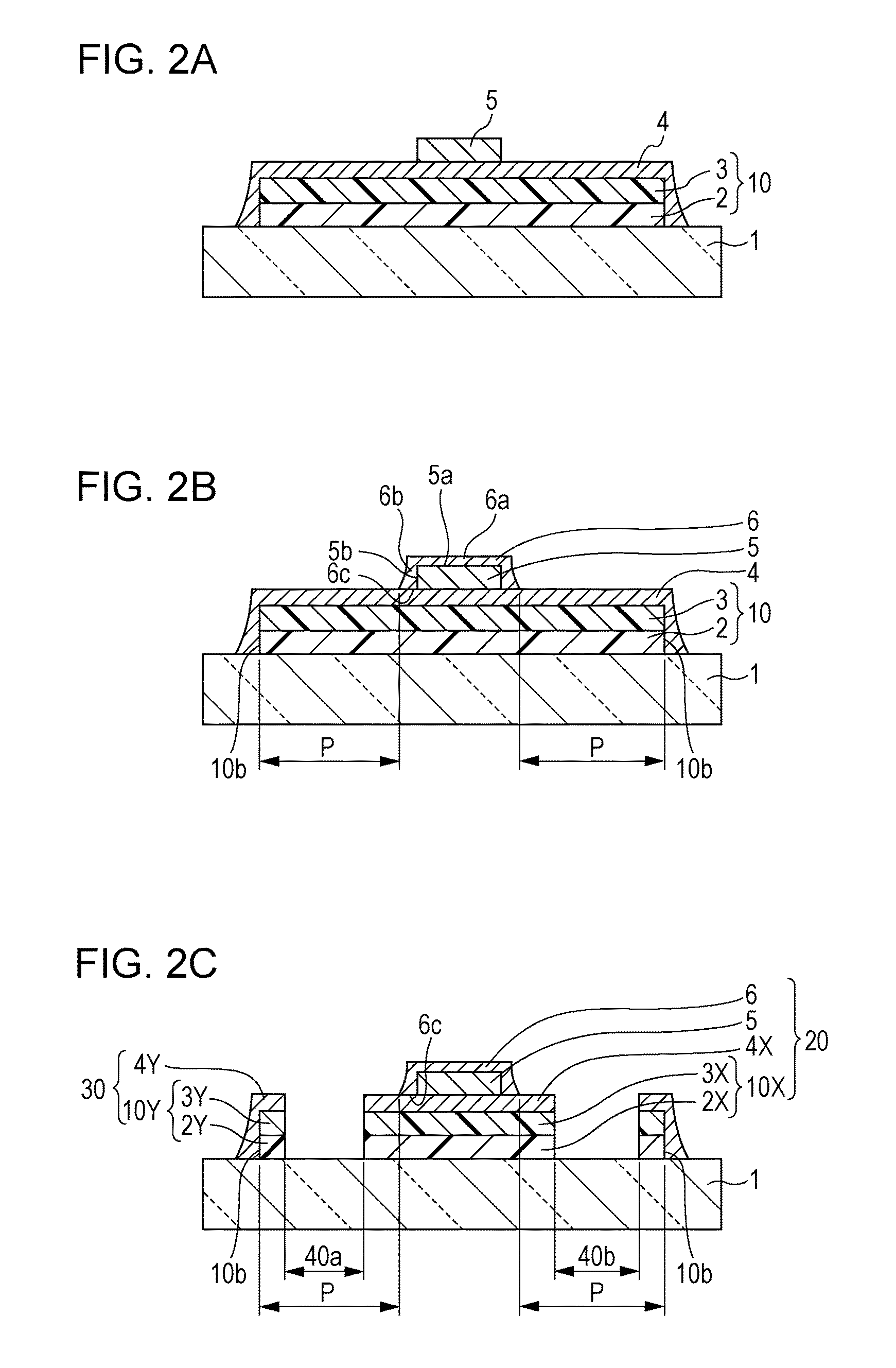
[0053]First, as shown in FIG. 1A, a support substrate 1 is prepared (Step S1). The support substrate 1 is used to preferably handle an in-process electronic device (hereinafter referred to as “intermediate electronic device product”), for example, in a process for manufacturing an electronic device. Hence, the support substrate 1 may have a strength so as to carry the intermediate electronic device product. As a material of the support substrate 1, for example, there may be used a glass material, such as non-alkali glass (borosilicate glass), alkali glass, soda glass, non-fluorescent glass, phosphoric acid-based glass, boric acid-based glass, or quartz, or an insulating material, such as alumina.
[0054]In order to i...
embodiment 2
[0080]In the embodiment 1, the case in which one electronic element 5 is formed on one resin layer 3 has been described.
[0081]In this embodiment, the case in which a plurality of electronic elements 5 is formed on one resin layer 3 will be described. In addition, the same constituent element as that described above is designated by the same reference numeral, and description thereof will be omitted.
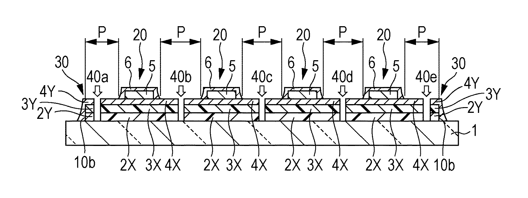
[0082]FIG. 9B shows the state in which after sets each including the second sealing layer 6 and the electronic element 5 are arranged in a 4×5 matrix on the first sealing layer 4, cutting is performed. FIG. 9A is a cross-sectional view taken along the line IXA-IXA of FIG. 9B. In this embodiment, the region P includes not only regions each located between the peripheral surface of the adhesive layer 2 and the second sealing layer 6 but also regions between adjacent second sealing layers 6. The reason for this is that also in the regions each located between adjacent second sealing layers 6...
modification examples of embodiments
Other Modification Examples of Embodiments
[0088](1) In the embodiments 1 and 2, although the first sealing layer 4 and the laminate structure 10 are collectively cut out by a cutter in Step S7, the present disclosure is not necessarily limited to this case. The cutting method may be performed either by a physical technique using a cutter or the like or by a chemical technique using etching or the like. In addition, the cutting depth required when the adhesive layer 2 is exposed is not limited to the case in which the first sealing layer 4, the resin layer 3, and the adhesive layer 2 are completely cut out, and as long as the first sealing layer 4 and the resin layer 3 are completely cut out, a part or the whole of the adhesive layer 2 may not be completely cut out. In addition, the support substrate 1 may be partially ground away instead of cutting the first sealing layer 4, or if the support substrate 1 is formed of a fragile material, such as a glass, cracks may be formed therein....
PUM
 Abstract
Description
Claims
Application Information


