

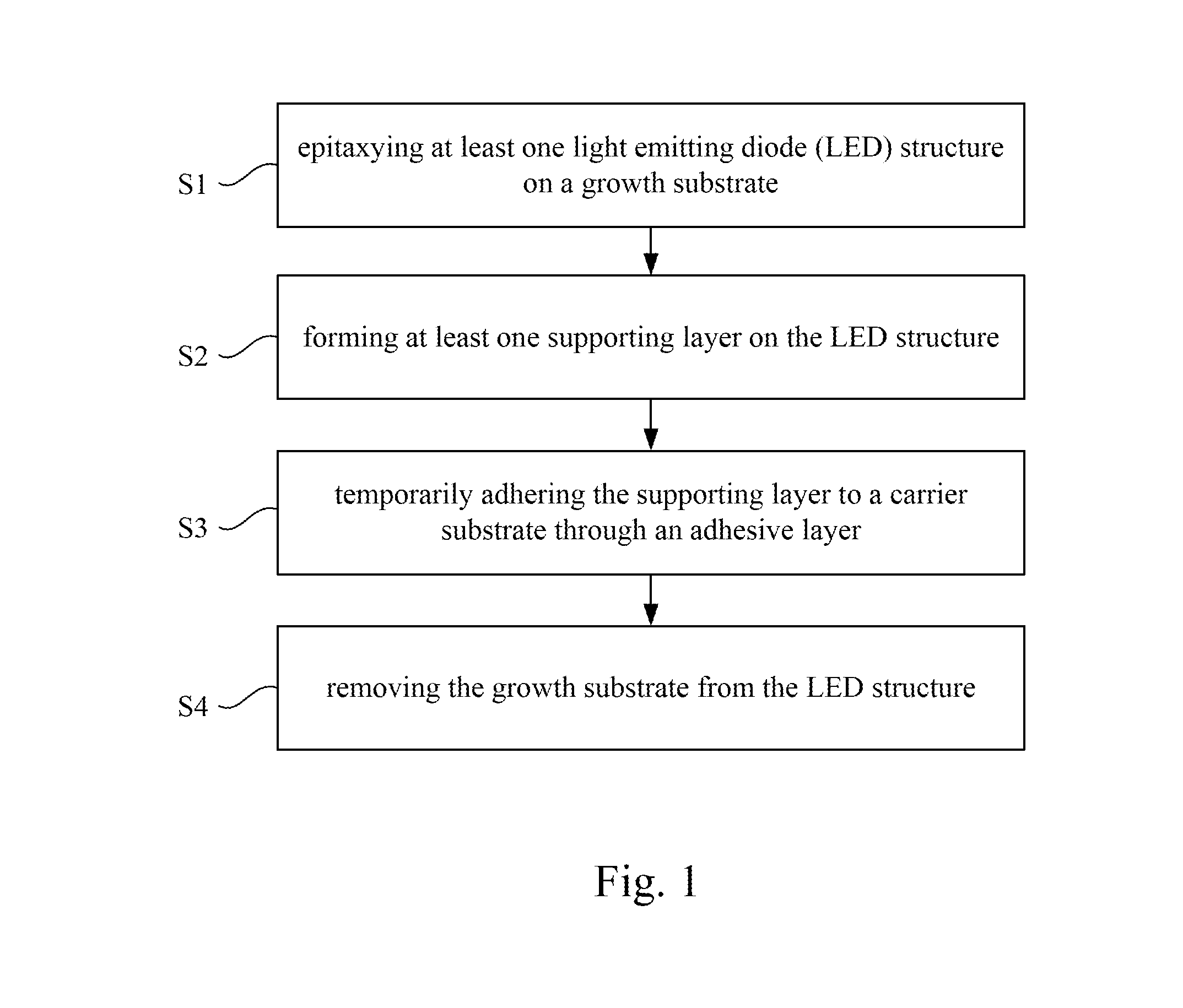
Method manufacturing light emitting diode having supporting lay7er attached to temporary adhesive
- Summary
- Abstract
- Description
- Claims
- Application Information
AI Technical Summary
Benefits of technology
Problems solved by technology
Method used
Image

Examples
Embodiment Construction
[0031]In the following detailed description, for purposes of explanation, numerous specific details are set forth in order to provide a thorough understanding of the disclosed embodiments. It will be apparent, however, that one or more embodiments may be practiced without these specific details. In other instances, well-known structures and devices are schematically shown in order to simplify the drawing.
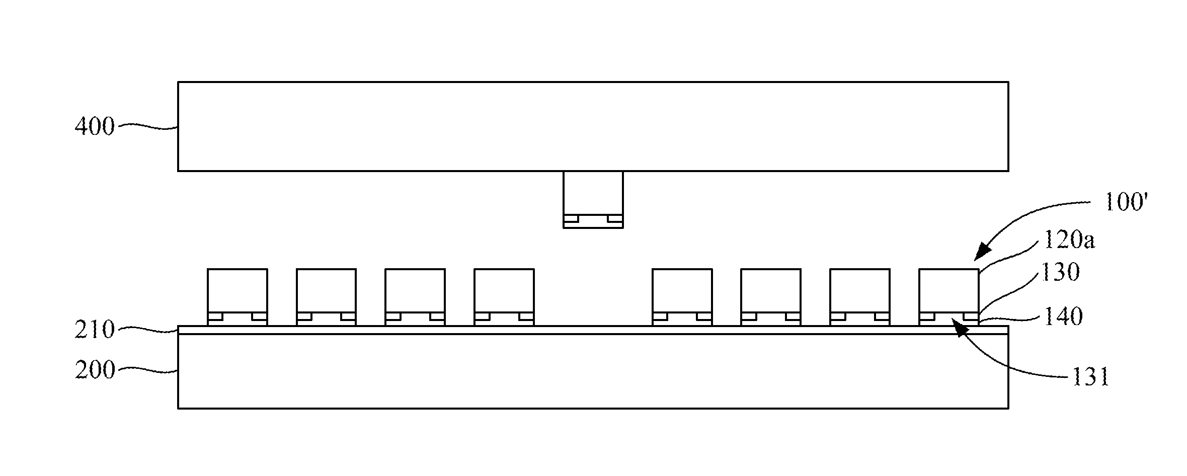
[0032]Embodiments of the present invention describe micro semiconductor devices such as micro-light-emitting diodes (micro-LEDs) and a method of removing a growth substrate of a semiconductor wafer and forming an array of micro semiconductor devices for transfer to a receiving substrate. For example, the receiving substrate may be, but is not limited to, a display substrate.
[0033]In various embodiments, description is made with reference to figures. However, certain embodiments may be practiced without one or more of these specific details, or in combination with other known methods...
PUM
 Abstract
Description
Claims
Application Information