In-plane switching LCD device

Inactive Publication Date: 2005-02-08
LG DISPLAY CO LTD
View PDF4 Cites 11 Cited by
  • Summary
  • Abstract
  • Description
  • Claims
  • Application Information

AI Technical Summary

Benefits of technology

Accordingly, the present invention is directed to an IPS LCD device that substantially obv

Problems solved by technology

However, the above-mentioned operation mode of the TN LCD panel has a disadvantage of a narrow viewing angle.
However, because the pixel and common electrodes are disposed on the same plane of the lower substrate, the transmittance and aperture ratio are low.
In addition, the IPS LCD device has disadvantages of a relatively slow response time and a relatively small alignment margin.
In case of the IPS LCD device, because the common line has a relatively high resistance, it is associated with a relatively high voltage drop.
Even if the common voltage signal is adjusted or compensated at an exterior drive circuit, the above-mentioned voltage drop cannot be avoided.
The voltage variation due to the voltage drop of the common voltage signal causes fatal defects, for example, a flicker to display quality of the conventional IPS LCD device.
Together with the above-mentioned voltage variation of the common voltage signal, a conventional structure of an inverted-staggered type TFT itself is associated with the flicker problem.
Specifically, the overlapping width of the drain electrode over the gate electrode is associated with the flicker problem.
Accordingly, the kickback voltage “ΔVp” cannot be compensated for sufficiently, and, thus, the flicker problem occurs in the IPS LCD device.

Method used


Image

  • In-plane switching LCD device
  • In-plane switching LCD device
  • In-plane switching LCD device

Examples


Embodiment Construction

Reference will now be made in detail to the preferred embodiments of the present invention, examples of which are illustrated in the accompanying drawings.

In an IPS LCD device according to the preferred embodiment, an overlapping width of a drain electrode varies in accordance with a position of a corresponding pixel region. Thereby, variation of a kickback voltage “ΔVp “(delta_Vp)” with respect to the position of the pixel region is minimized and a flicker problem of the IPS LCD device is avoided.

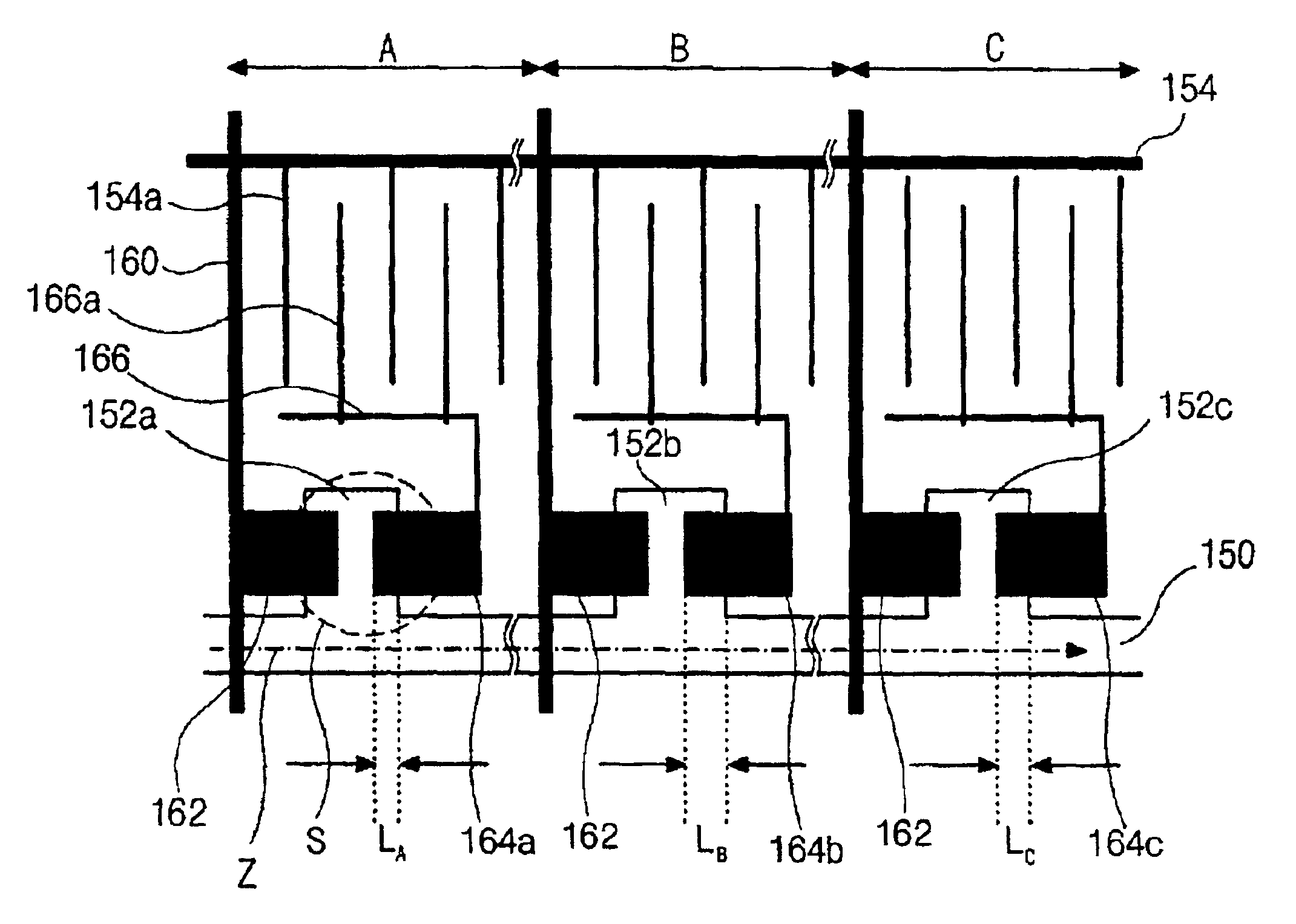
In FIG. 9, a first pixel region “A” and a third pixel region “C” are arranged at a left side and at a right side, respectively, with a second pixel region “B” disposed therebetween. In the pixel region “A” (“B”, “C”), a gate line 150 and a common line 154 are arranged parallel to each other, and a data line 160 is arranged perpendicular to the gate and common lines 150 and 154. Near a cross point of the gate and data lines 150 and 160, a gate electrode 152a (152b, 152c) and a source electr...


PUM


Abstract

The present invention concerns a liquid crystal display device including: a substrate; a plurality of thin film transistors each including a gate electrode, a source electrode, and a drain electrode; a gate line and a data line electrically connecting with the gate electrode and the source electrode, respectively; and a pixel electrode electrically connecting with the drain electrode, wherein overlapping widths between the gate electrode and the source and drain electrodes vary in accordance with the position of the thin film transistor.

Description

This application claims the benefit of Korean Patent Applications No. 2000-42533 filed on Jul. 24, 2000, which is hereby incorporated by reference as if fully set forth herein.BACKGROUND OF THE INVENTION1. Field of the InventionThe present invention relates to a liquid crystal display device, and more particularly to a liquid crystal display device implementing in-plane switching (IPS) where an electric field to be applied to liquid crystal is generated in a plane parallel to a substrate.2. Discussion of the Related ArtA typical liquid crystal display (LCD) device uses optical anisotropy and polarization properties of liquid crystal molecules. The liquid crystal molecules have a definite orientational order in alignment resulting from their thin and long shapes. The alignment of the liquid crystal molecules can be controlled by supplying an electric field to the liquid crystal molecules. In other words, as the alignment direction of the electric field is changed, the alignment of th...

Claims


Application Information

Patent Timeline
IPC IPC(8): G02F1/13G02F1/1368G02F1/1343G02F1/136
CPCG02F1/134363G02F1/1368G02F1/136286G02F2001/13606G02F1/13606G02F1/136
Inventor LEE, JOUN-HOKO, DOO-HYUN
Owner LG DISPLAY CO LTD
Why Eureka
Try Eureka