Automatically adjustable wafer probe card

Inactive Publication Date: 2005-02-15
TAIWAN SEMICON MFG CO LTD
View PDF4 Cites 22 Cited by
  • Summary
  • Abstract
  • Description
  • Claims
  • Application Information

AI Technical Summary

Benefits of technology

Each of the probe needles is typically mounted on a corresponding needle mount block that is engaged by a corresponding needle drive motor and a pinion gear. The teeth of the pinion gear mesh with teeth in the shift block, and the motor is driven to rotate the pinion gear and facilitate travel of the probe needle along a pitch shift channel in the shift block. A micro-precision stepping motor control system interfaces with the needle drive motors of the respective probe needl

Problems solved by technology

Because the ink marking process can be messy and introduce possible contaminants onto the chip, electronic wafer maps are increasingly being used to create a computer image of chip location and test results to categorize good and bad die on the wafer.
The reduction in size and increase in density of the probe needles has inevitably made the manufacture and mounting of the needles on the probe card troublesome.
These variations in probe n

Method used


Image

  • Automatically adjustable wafer probe card
  • Automatically adjustable wafer probe card
  • Automatically adjustable wafer probe card

Examples


Embodiment Construction

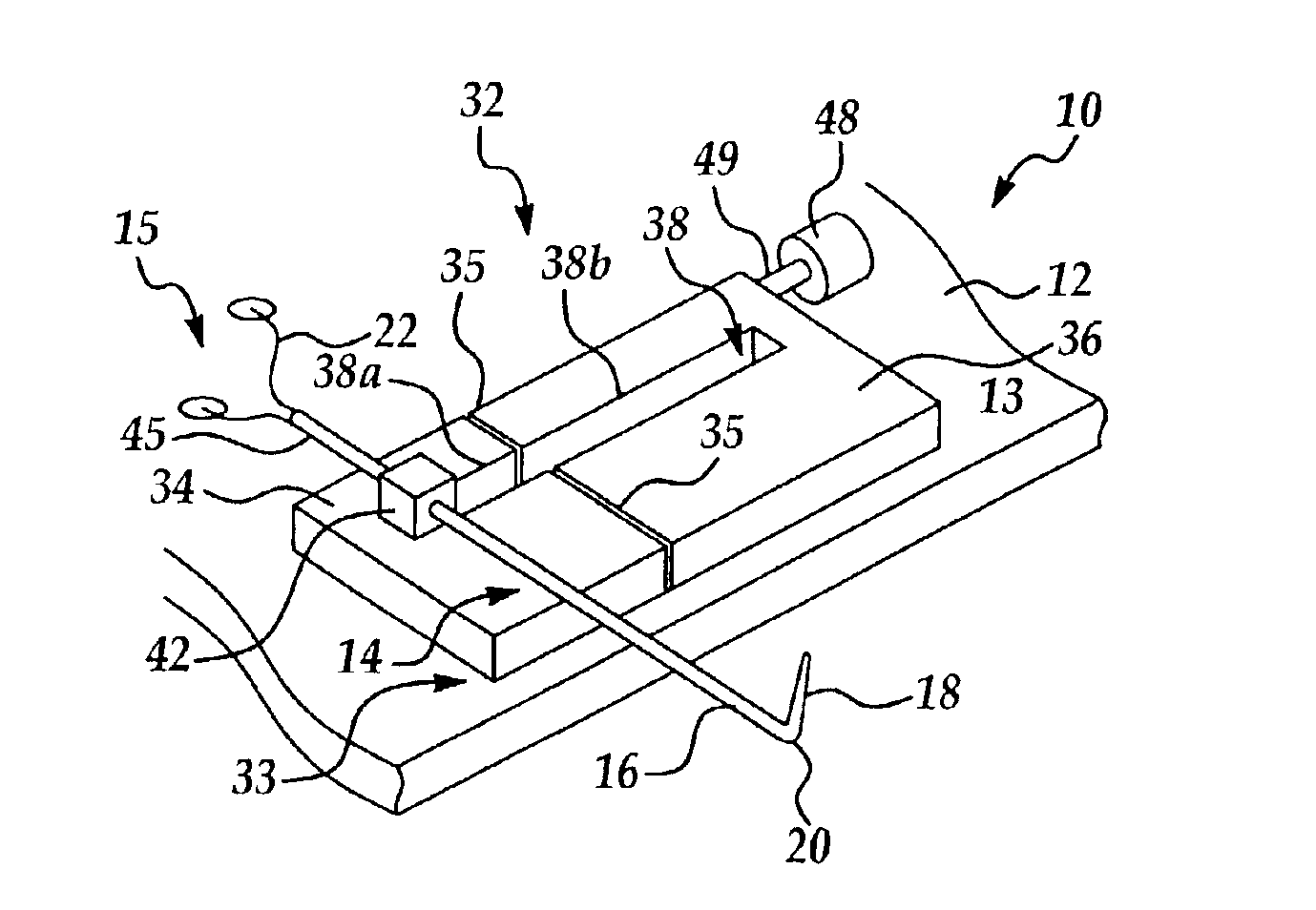
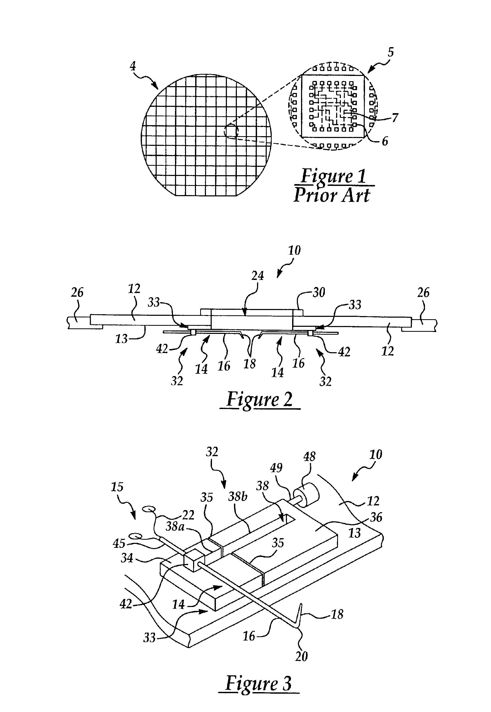
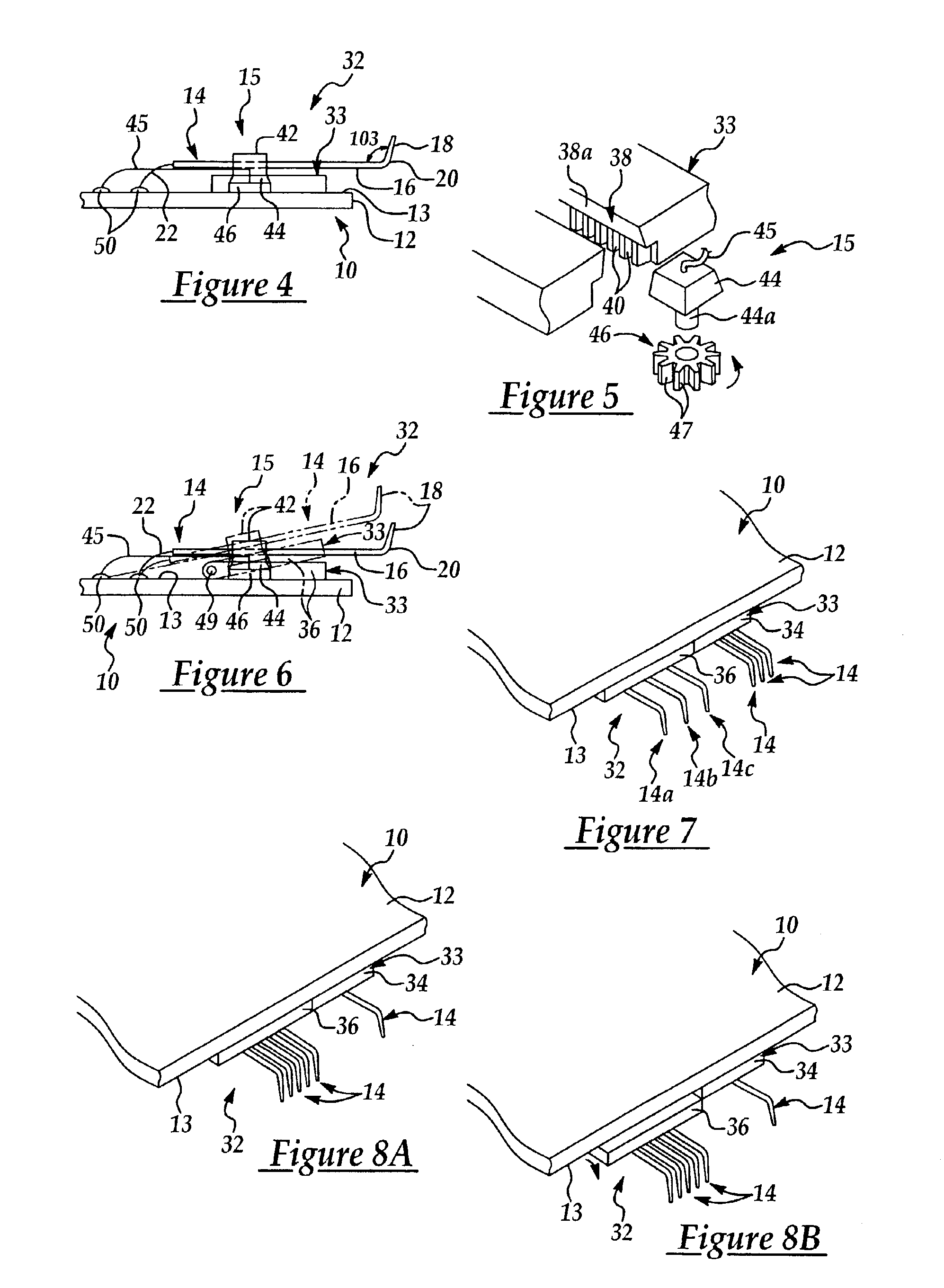
Referring initially to FIGS. 2-8B, the present invention relates to a wafer probe card 10 having multiple probe needles 14, the number, pitch and height of which may be automatically adjusted to make electrical contact with elements on a microelectronic device such as an integrated circuit, depending on the particular testkey configuration of the device to be tested. The probe needle configuration of the wafer probe card 10 can be quickly and automatically changed for testing of successive devices having different testkey configurations, as hereinafter described. As shown in FIG. 2, the probe card 10 generally includes a planar board 12 having a central opening or cut-out 24 therein which is typically square or rectangular in shape. The board 12 may be formed of conventional printed circuit board materials, as well as other suitable materials which are electrically insulative. The probe card board 12 fits within and is supported on a stage 26 which is vertically movable relative to ...


PUM


Abstract

An automatically adjustable wafer probe card for the testing of integrated circuits fabricated on a wafer. The wafer probe card includes a pitch shift assembly having a shift block that includes a reserve needle block and an adjacent functional needle block. Multiple probe needles are linearly adjustable on the shift block, and a selected number of the probe needles can be shifted from the reserve needle block to the functional needle block depending on the number of contact pads on the integrated circuit to be contacted by the probe needles of the wafer probe card during the testing process. A selected spacing between the probe needles, or pitch, can be achieved by locating the probe needles at the selected spacings from each other along the functional needle block.

Description

FIELD OF THE INVENTIONThe present invention relates to wafer probe cards used in testing electrical characteristics of integrated circuits fabricated on a semiconductor wafer substrate. More particularly, the present invention relates to a wafer probe card having a probe needle number and probe needle pitch that are automatically selectable to accommodate test keys of various design.BACKGROUND OF THE INVENTIONA conventional method used by the semiconductor industry in the manufacturing of semiconductor integrated circuits includes the steps of fabrication, wafer sort, assembly and test, respectively. As shown in FIG. 1, in the fabrication step, as many as several thousand dies (integrated circuits) 5 are formed onto a semiconductor wafer 4. In the wafer sort step, each of the dies 5 on the wafer 4 is tested to determine its electrical characteristics and operability, and defective dies are distinguished from operable dies. The defective dies are often marked by an ink mark at the wa...

Claims


Application Information

Patent Timeline
IPC IPC(8): G01R1/073
CPCG01R1/07392
Inventor LIANG, SHENG-HUILOU, CHINE-GIE
Owner TAIWAN SEMICON MFG CO LTD
Why Eureka
Try Eureka