

Method for fabricating semiconductor packages with stacked dice and leadframes
a technology of semiconductor packages and leadframes, which is applied in the direction of semiconductor devices, semiconductor/solid-state device details, electrical equipment, etc., can solve the problems of complex fabrication process, inefficient transfer of dice heat generated by multiple dice packages, and lead frame with die mounting paddles
- Summary
- Abstract
- Description
- Claims
- Application Information
AI Technical Summary
Benefits of technology
Problems solved by technology
Method used
Image

Examples
Embodiment Construction
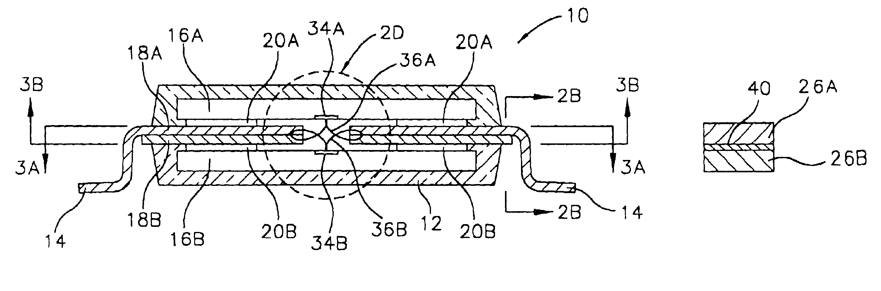
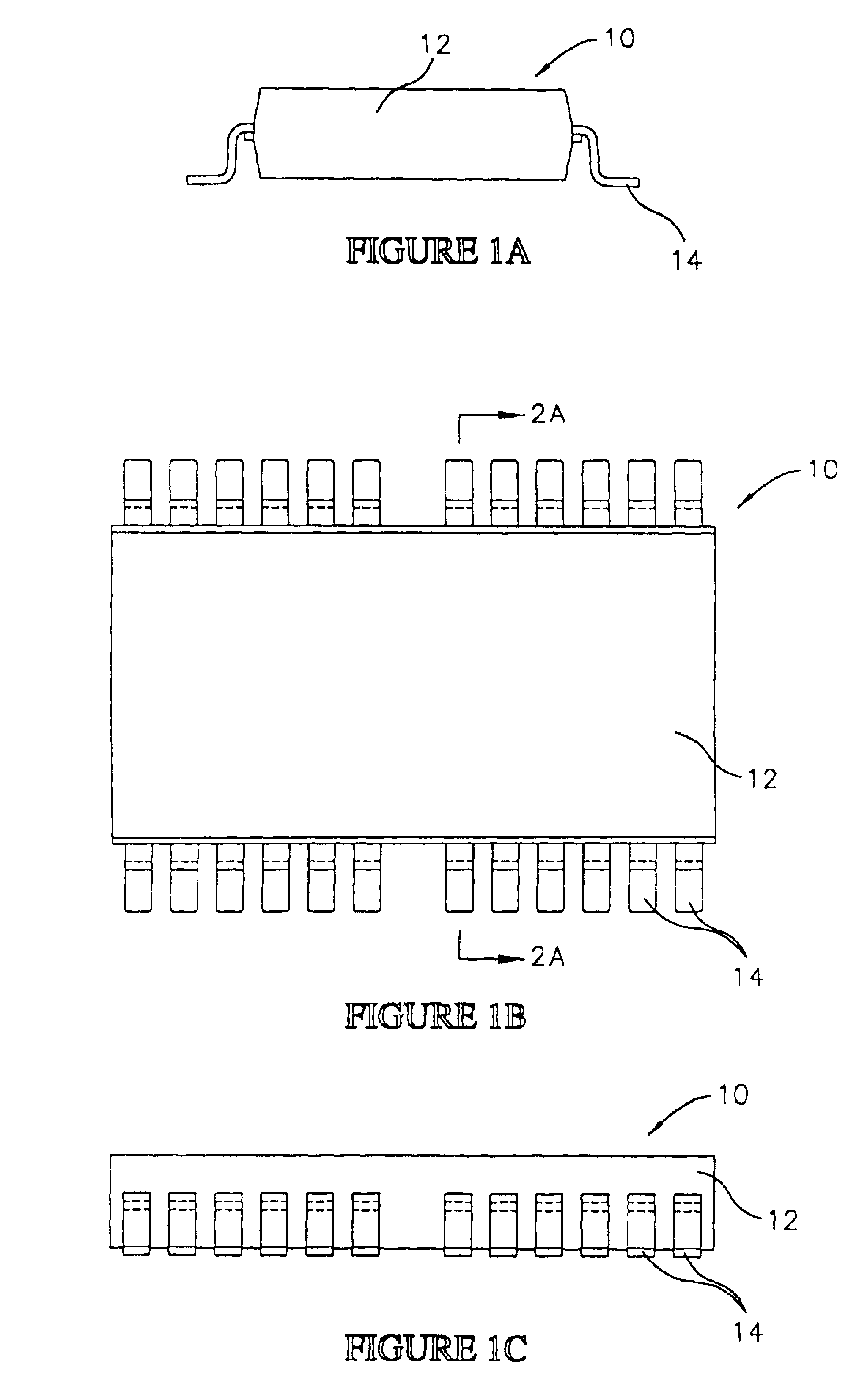
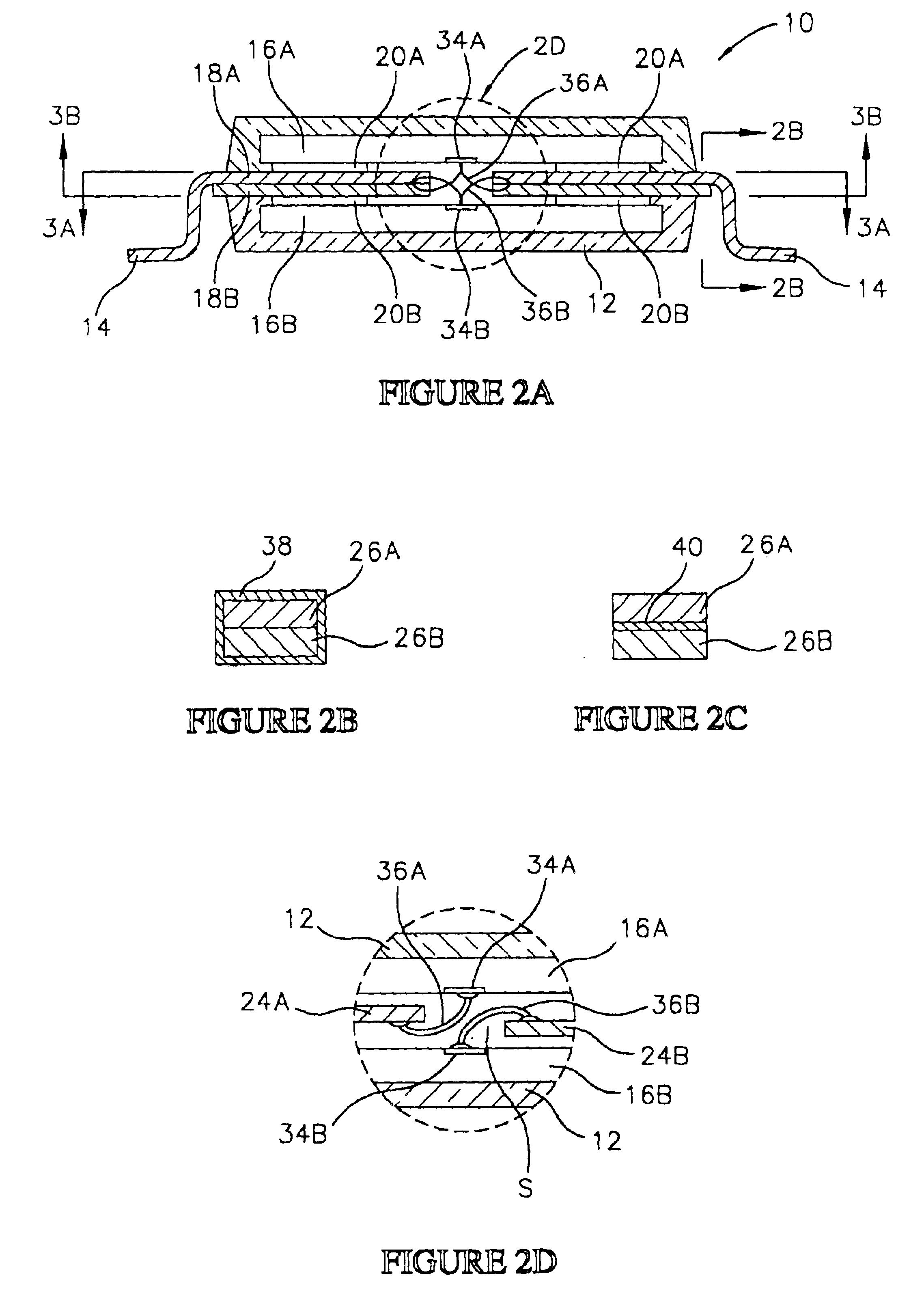
Referring to FIGS. 1A-1C, a semiconductor package 10 constructed in accordance with the invention is illustrated. In the illustrative embodiment the package 10 has the configuration of a thin small outline package (TSOP). Alternately, the package 10 can have any other conventional configuration such as DIP (dual in line package), ZIP (zig zag in line package), LCC (leadless chip carrier), SOP (small outline package), QFP (quad flat pack), and SOJ (small outline j-bend).
The package 10 includes a plastic body 12 and a plurality of terminal leads 14 extending from the body 12. The terminal leads 14 are in electrical communication with the integrated circuits (not shown) contained within the package 10, and form separate electrical paths from the outside to the integrated circuits. In the illustrative embodiment, the terminal leads 14 have a gull-wing configuration to permit surface mounting of the package 10 to mating electrodes on a supporting substrate, such as a printed circuit boar...
PUM
 Abstract
Description
Claims
Application Information