

Digital signal processor computation core with pipeline having memory access stages and multiply accumulate stages positioned for efficient operation
a technology of computation core and pipeline, applied in the field of digital signal processor computation core architecture, can solve the problems of high interrupt rate and intensive numeric computation, the architecture optimized for dsp computation typically does not operate efficiently as microcontroller, and the architecture optimized for dsp computation tends to be intensive, so as to achieve efficient digital signal computation and high code storage density
- Summary
- Abstract
- Description
- Claims
- Application Information
AI Technical Summary
Benefits of technology
Problems solved by technology
Method used
Image

Examples
first embodiment
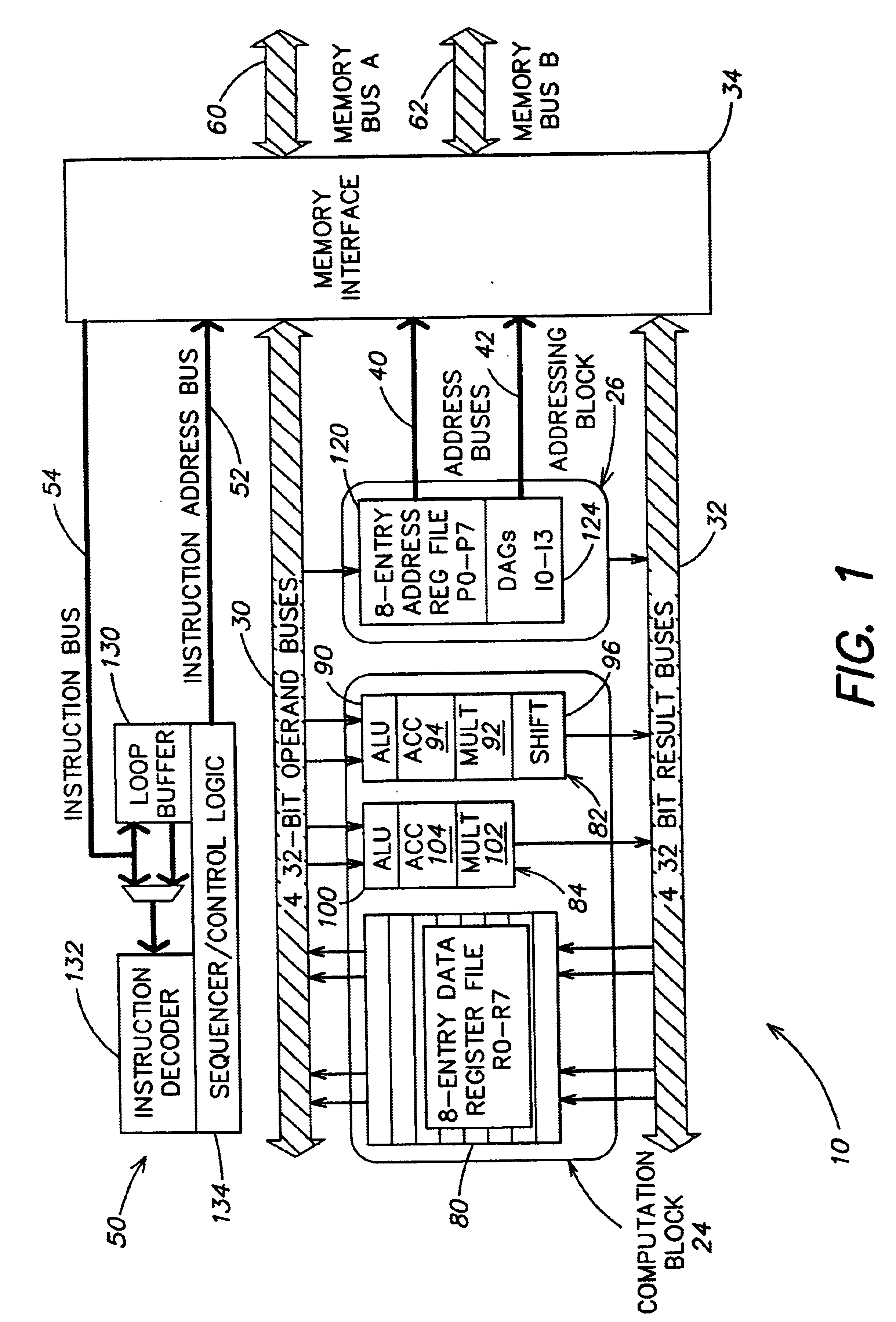
A block diagram of register file 80, execution units 82 and 84 and memory 64, and the interconnection between these elements, is shown in FIG. 3. In the embodiment of FIG. 3, register file 80 has eight registers and is partitioned into register file banks 200 and 202, each having four registers of 32 bits each. Thus, register file bank 200 contains registers R0-R3, and register file bank 202 contains registers R4-R7. This arrangement results in low power because each four entry register file bank 200, 202 requires less energy per access than a single eight entry register file. Each four entry register file bank 200, 202 requires two read ports and two write ports, while an eight entry register file requires four read ports and four write ports.
Register file 80 is connected to execution units 82 and 84 and to memory 64 by operand buses 30 and result buses 32. Operand buses 30 include operand bus 210, operand bus 212, operand bus 214 and operand bus 216. Operand buses 210 and 212 are ...
second embodiment
A block diagram of register file 80, execution units 82 and 84 and memory 64, and the interconnection between these elements, is shown in FIG. 3A. Like elements in FIGS. 3 and 3A have the same reference numerals. In the embodiment of FIG. 3A, register file 80 has a single register file bank 240 having eight registers, R0-R7, of 32 bits each. Register file bank 240 has four read ports and four write ports.
A block diagram of execution units 82 and 84 is shown in FIG. 4. A portion of execution unit 82 is shown in more detail in FIG. 4A. Execution unit 82 includes a multiplier array 250, an ALU 252, an accumulator 254 and a barrel shifter 256. Execution unit 84 includes a multiplier array 260, an ALU 262 and an accumulator 264. Each multiplier array 250, 260 receives two 16-bit operands and provides two 32-bit outputs to the respective ALUs 252, 262. ALUs 252 and 262 may also receive two 32-bit inputs from operand buses 214 and 216. In a preferred embodiment, ALUs 252 and 262 are 40-bit...
PUM
 Abstract
Description
Claims
Application Information