

Integrated circuit burn-in test system and associated methods
a test system and integrated circuit technology, applied in the direction of electronic circuit testing, measurement devices, instruments, etc., can solve the problems of limited throughput of burn-in chambers, slow and expensive test in burn-in chambers, etc., and achieve the effect of straightforward devices
- Summary
- Abstract
- Description
- Claims
- Application Information
AI Technical Summary
Benefits of technology
Problems solved by technology
Method used
Image

Examples
Embodiment Construction
The present invention will now be described more fully hereinafter with reference to the accompanying drawings, in which preferred embodiments of the invention are shown. This invention may, however, be embodied in many different forms and should not be construed as limited to the embodiments set forth herein. Rather, these embodiments are provided so that this disclosure will be thorough and complete, and will fully convey the scope of the invention to those skilled in the art. Like numbers refer to like elements throughout and prime and multiple prime notations are used in alternate embodiments.
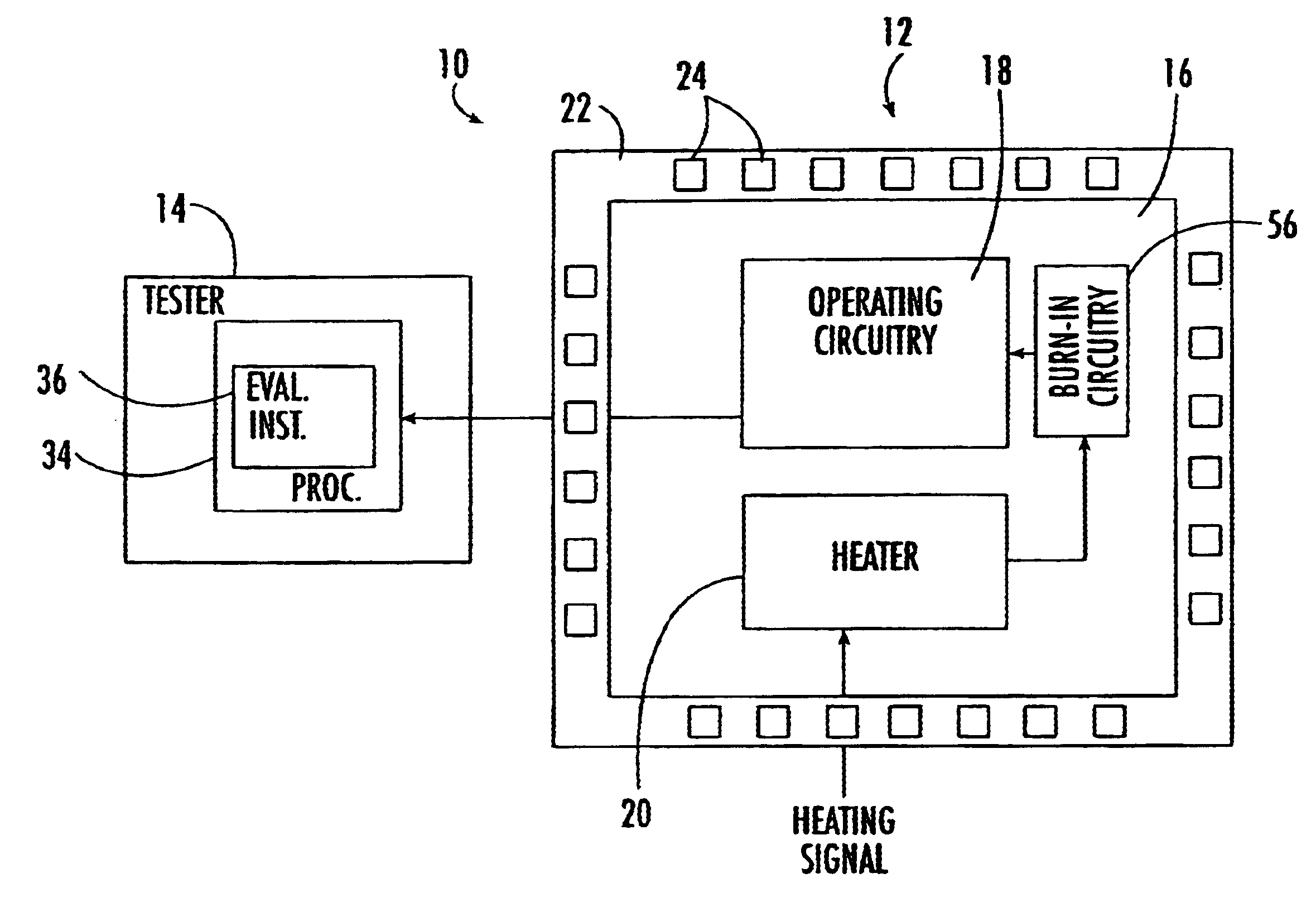
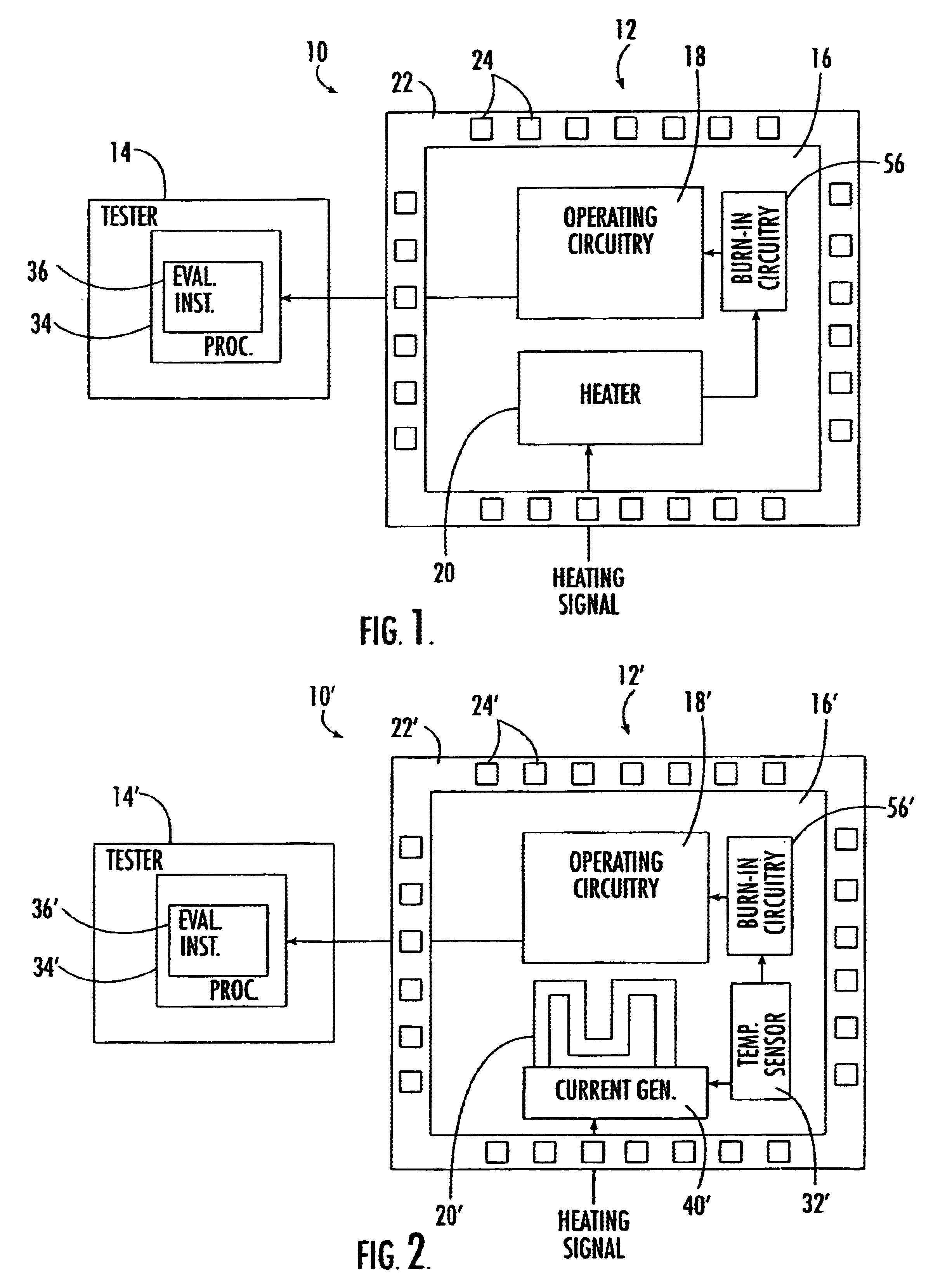
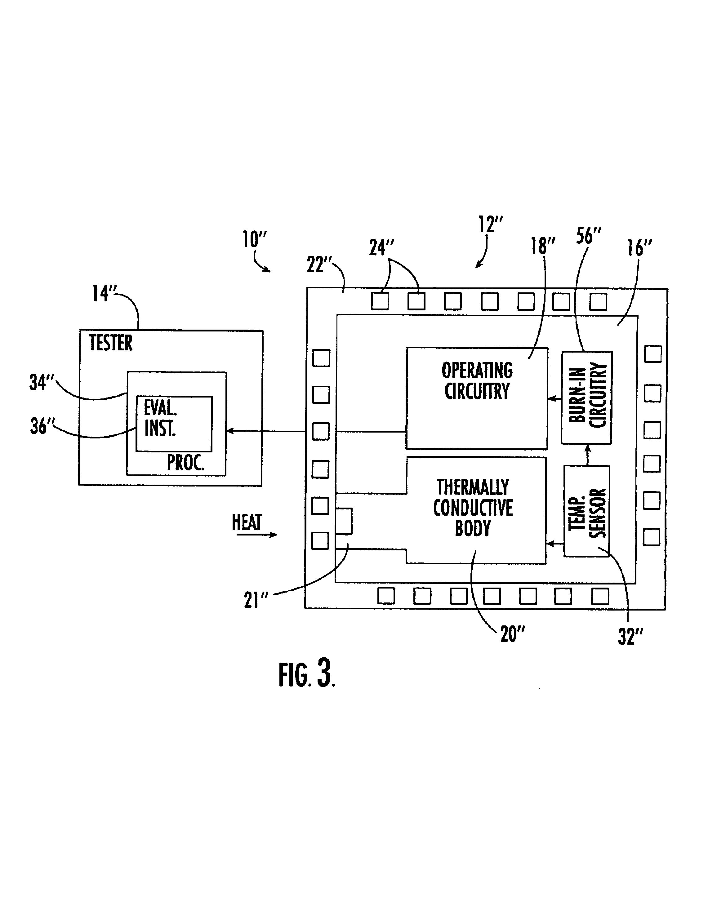
Referring initially to FIGS. 1-3, an integrated circuit burn-in test system 10 in accordance with the present invention will be described. The test system 10 includes an integrated circuit 12 and a tester 14 therefor. The integrated circuit 12 includes operating circuitry 18, a heater 20 for heating the operating circuitry, and burn-in test circuitry 56 for testing the operating circuitry w...
PUM
 Abstract
Description
Claims
Application Information