Monolithic, combo nonvolatile memory allowing byte, page and block write with no disturb and divided-well in the cell array using a unified cell structure and technology with a new scheme of decoder and layout

a combination nonvolatile memory and cell array technology, applied in the field of new combination nonvolatile memory and a novel embedded memory, can solve the problems of large overhead in the cell array area, the 2tr-flotox eeprom suffers a big penalty in cell size and cell array area, and the traditional flash memory is less flexible than. , to achieve the effect of reducing the area-consuming divided triple-well, superior combo, and nonvolatile memory

Inactive Publication Date: 2005-03-01
CALLAHAN CELLULAR L L C
View PDF11 Cites 128 Cited by
  • Summary
  • Abstract
  • Description
  • Claims
  • Application Information

AI Technical Summary

Benefits of technology

The present invention overcomes all the above said drawbacks in 2Tr-FLOTOX-EEPROM, Toshiba's 3Tr-NAND and 4Tr-NAND and other similar FLASH-based EEPROM technologies. A novel FLASH-based EEPROM cell, decoder, and layout scheme are disclosed to eliminate the area-consuming divided triple-well in cell array and allows byte-erase and byte-program for high P / E cycles. Furthermore, the process-compatible FLASH cell for EEPROM part can be integrated with FLASH and ROM parts so that a superior combo, monolithic, nonvolatile memory is achieved. Unlike all previous arts, the novel combo nonvolatile memory of the present invention of ROM, EEPROM and FLASH or combination of any two is made of one unified, fully compatible, highly-scalable BN+cell and unified process. In addition, its cell operation schemes have zero array overhead and zero disturbance during P / E operations. The novel combo nonvolatile memory is designed to meet the need in those markets requiring flexible write size in units of bytes, pages and blocks at a lower cost.
Yet another further object of the present invention is to provide a nonvolatile cell that is comprised of 2Tr BN+S / D as derived from FLASH OR-array proposed by the same inventors of the present invention for minor bitline disturb and zero wordline disturb during byte-erase and byte-program operations to further reduce cell and array size.
Yet another further object of the present invention is to provide a novel zero-disturb column-decoder scheme and unique layout techniques that vertically output a plurality of metalline buses connecting to the selected wordline in units of bytes in BN+cell array to completely eliminate the vertically divided triple well on byte basis in Toshiba's 3Tr-NAND or 4Tr-NAND cell structures as well as other similar byte-writable cell arrays.
A further object of the present invention is to provide novel schemes of zero-disturb column-decoders, row-decoders and unique layout techniques that output a plurality of metalline buses running vertically or horizontally, connecting to the selected wordline in units of bytes in Toshiba's 3Tr-NAND or 4Tr-NAND arrays to completely eliminate Toshiba's and other's vertically divided triple well for byte-writable arrays.
Still another object of the present invention is to provide novel schemes of zero-disturb column-decoders, row-decoders and unique layout techniques that output a plurality of metalline buses running vertically or horizontally, connecting to the selected wordline in units of bytes in 1Tr-ETOX array to completely eliminate any divided triple well for byte-writable arrays.
A further object of the present invention is to provide novel schemes of split operating voltages of zero-disturb column-decoders, row-decoders and unique layout techniques that output a plurality of metalline buses running vertically or horizontally, connecting to the selected wordline in units of bytes in Toshiba's 3Tr-NAND and 4Tr-NAND arrays to completely eliminate their vertically divided triple well for byte-writable arrays. The split operating voltages of the present patent can further reduce P / E program voltages from 20 V to + / −10 V.

Problems solved by technology

For example, FLASH typically only performs page(128B) or block(64 KB) erase and page(128B) or byte(1B) program, while EEPROM requires byte(1B) erase and byte(1B) program, causing large overhead in the cell array area.
Traditional FLASH memory is less flexible than EEPROM in erase size, but 2Tr-FLOTOX EEPROM suffers a big penalty in cell size and cell array area.
There are two disadvantages that cause this larger cell size and cell array area of 2Tr-FLOTOX EEPROM.
The other disadvantage is the requirement of flexible byte erase and byte program, which results in an unique area consuming cell array architecture-divided wordline and divided bitline in units of bytes.
As a consequence, the total die area of Toshiba's proposed FLASH-based EEPROM still has a very large overhead.
This overhead is drastically increased as the cell geometry is shrunken smaller and smaller.

Method used


Image

  • Monolithic, combo nonvolatile memory allowing byte, page and block write with no disturb and divided-well in the cell array using a unified cell structure and technology with a new scheme of decoder and layout
  • Monolithic, combo nonvolatile memory allowing byte, page and block write with no disturb and divided-well in the cell array using a unified cell structure and technology with a new scheme of decoder and layout
  • Monolithic, combo nonvolatile memory allowing byte, page and block write with no disturb and divided-well in the cell array using a unified cell structure and technology with a new scheme of decoder and layout

Examples


Embodiment Construction

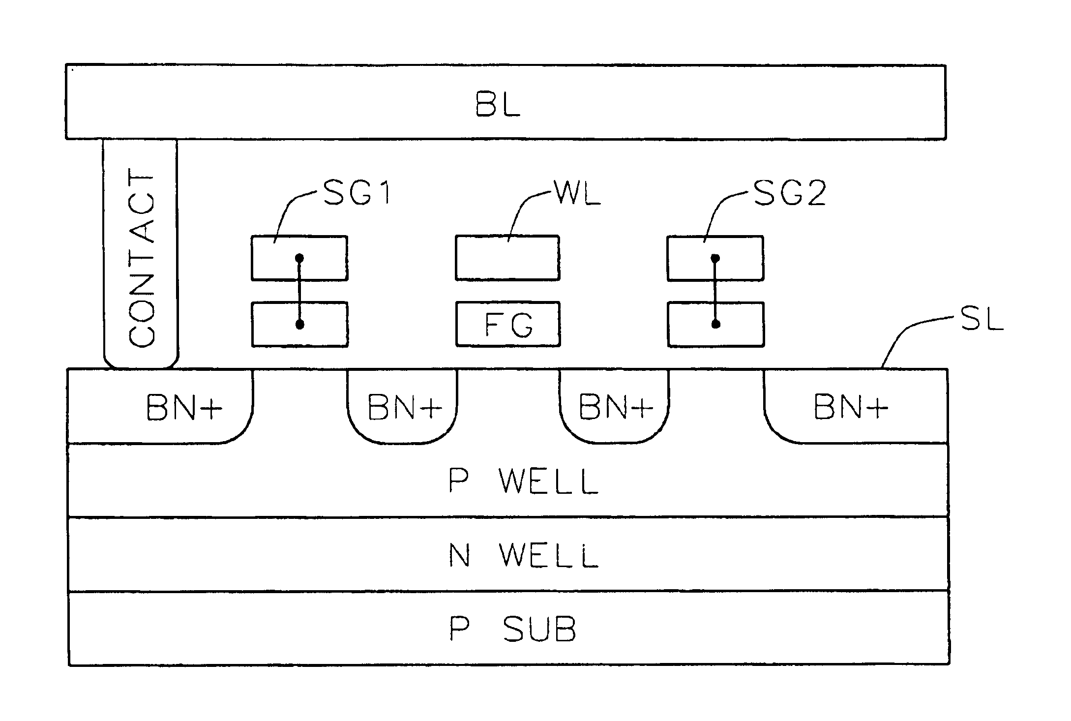
The present invention is a novel combo nonvolatile semiconductor memory and embedded memory that employs several new schemes of byte-wordline decoders and unique layout techniques associated with an unified, highly-scalable BN+S / D (Source / Drain) cell architecture with the same process for integrating FLASK EEPROM and ROM into one monolithic chip. The present invention will be described below in detail with reference to the accompanying drawings.

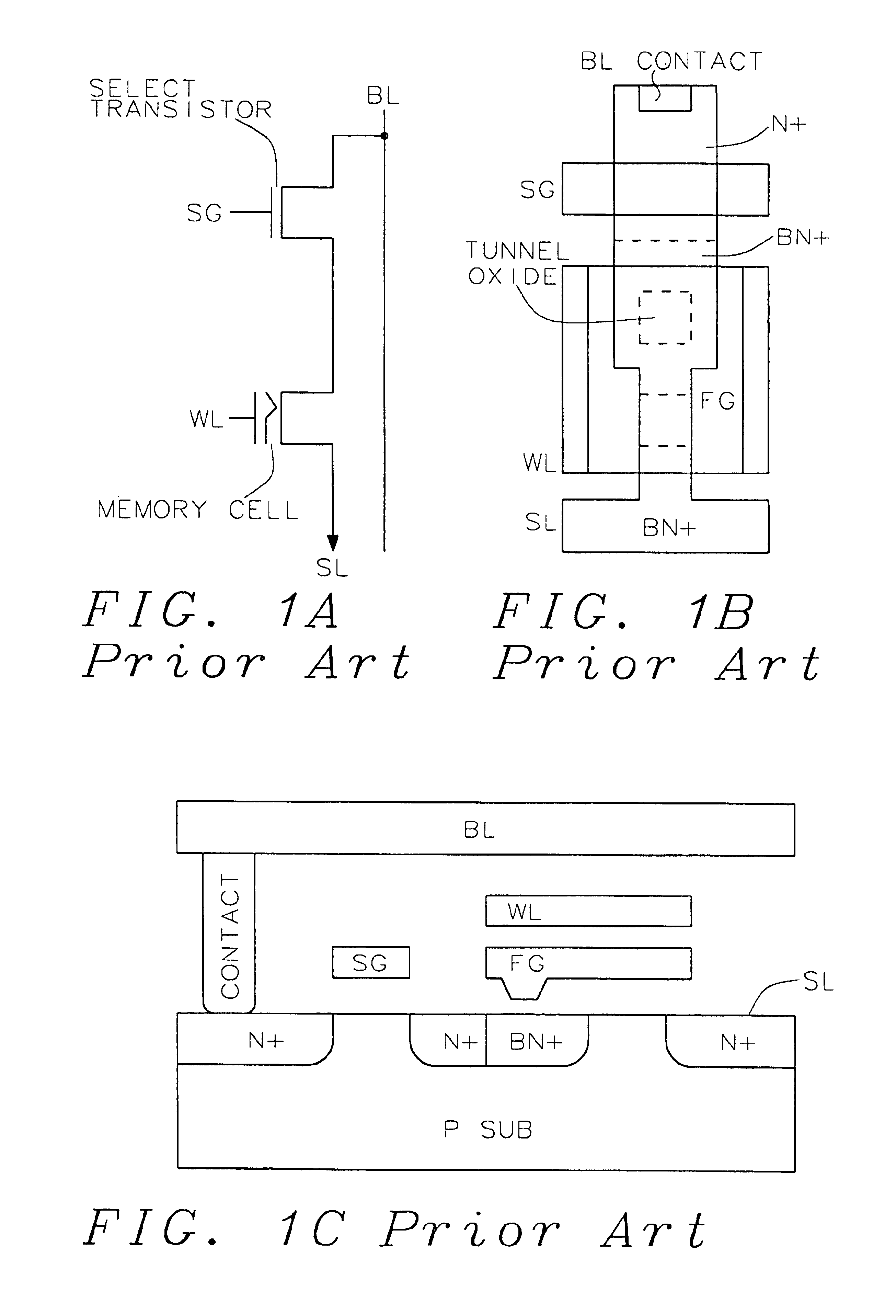
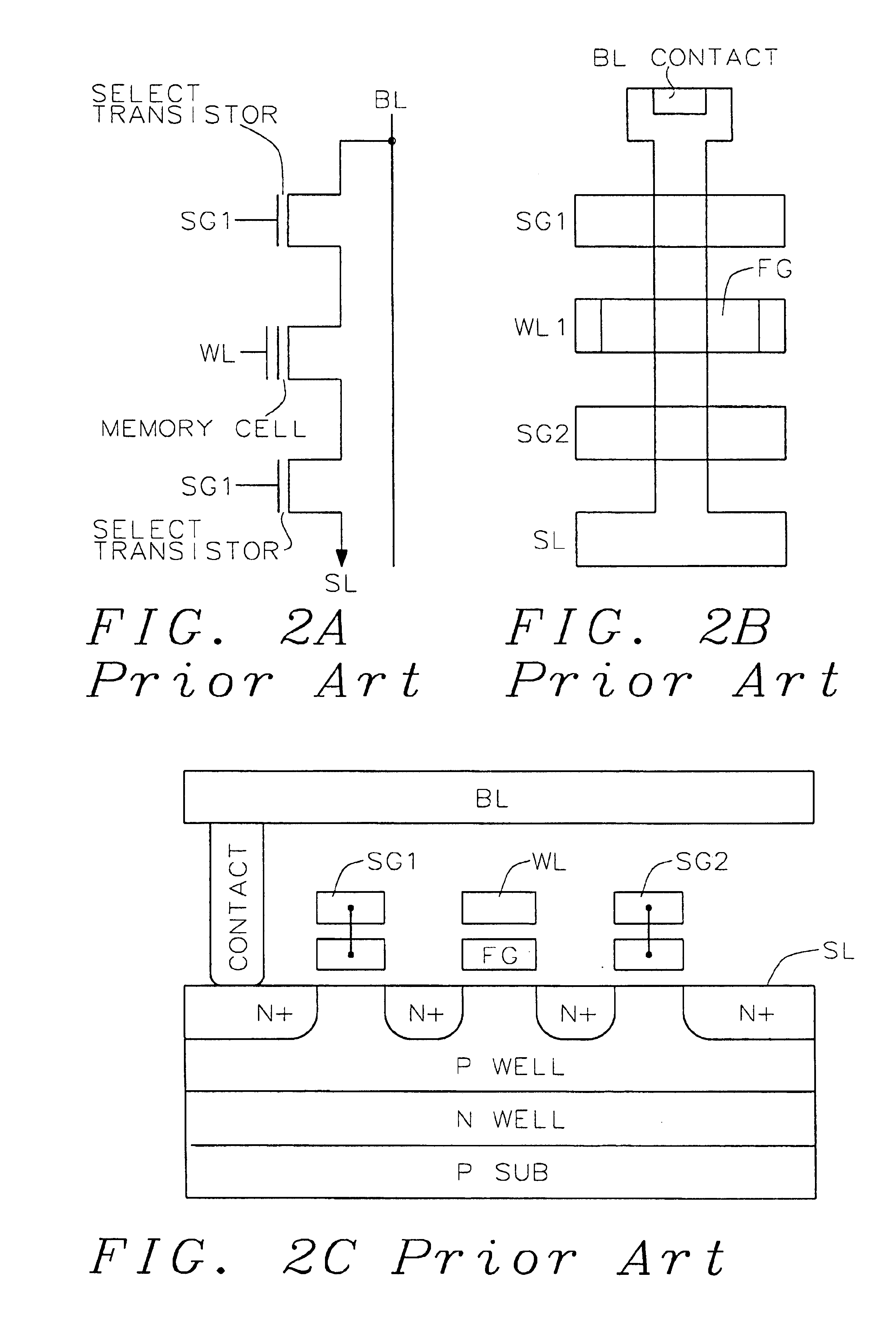
FIG. 1A, FIG. 1B and FIG. 1C illustrate a circuit schematic, top view of layout and the cross-sectional view of a prior art of conventional 2Tr-FLOTOX EEPROM cell. The 1st transistor is a n-channel select transistor with its gate connected to SG, drain connected to metal1(M1) bitline BL and source connected to the floating-gate, two-poly nonvolatile memory transistor with tunneling oxide surrounding by BN+as shown in FIG. 1B. The tunneling oxide thickness is designed to be around 100A and will have a FN-tunneling effect when 10 V is applied a...


PUM


Abstract

A novel FLASH-based EEPROM cell, decoder, and layout scheme are disclosed to eliminate the area-consuming divided triple-well in cell array and allows byte-erase and byte-program for high P / E cycles. Furthermore, the process-compatible FLASH cell for EEPROM part can be integrated with FLASH and ROM parts so that a superior combo, monolithic, nonvolatile memory is achieved. Unlike all previous arts, the novel combo nonvolatile memory of the present invention of ROM, EEPROM and FLASH or combination of any two is made of one unified, fully compatible, highly-scalable BN+cell and unified process. In addition, its cell operation schemes have zero array overhead and zero disturbance during P / E operations. The novel combo nonvolatile memory is designed to meet the need in those markets requiring flexible write size in units of bytes, pages and blocks at a lower cost.

Description

BACKGROUND OF THE INVENTION(1) Field of the InventionThe present invention relates to a novel combination nonvolatile memory and a novel embedded memory. The nonvolatile memory is comprised of three key memories: ROM (Read-Only-Memory), EEPROM (Electrically Erasable and Programmable Read Only Memory) and FLASH. The embedded memory is comprised of the combination of the above three nonvolatile memories, SRAM, CPU, and shared buses of data, address, and control signals.(2) Description of the Prior ArtROM data can only be altered at the manufacturing site by changing the costly photo mask sets, while both data of EEPROM and FLASH is allowed to be in-system flexibly changed at user's site at lower cost and faster throughput than ROM. The main differences in product specification requirements between FLASH and EEPROM are not the write scheme nor write speed but the write size and endurance cycles. Endurance cycle stands for the number of successful program and erase cycles when changing ...

Claims


Application Information

Patent Timeline
Patent Type & Authority Patents(United States)
IPC IPC(8): G11C16/04G11C11/34H01L27/115
CPCH01L27/11524G11C16/0416G11C16/0433G11C16/3436G11C16/344G11C16/3445G11C16/3454G11C16/3459H01L27/115H01L27/11519H01L27/11521G11C11/005G11C16/10G11C16/16G11C16/0408H10B41/10H10B69/00H10B41/30H10B41/35
Inventor LEE, PETER W.HSU, FU-CHANGTSAO, HSING-YAMA, HAN-REIWU, KOUCHENG
Owner CALLAHAN CELLULAR L L C
Why Eureka
Try Eureka