Method of forming bumps

a technology of bumps and bumps, which is applied in the direction of manufacturing tools, soldering devices, non-printed masks, etc., can solve the problems of not being able to properly connect all bumps between semiconductor devices, it is difficult in principle to form bumps of enough cubic volume, and it takes a long time to produce many pads. , to achieve the effect of low cost, fast production of bumps, and low cos

Inactive Publication Date: 2005-03-22
RENESAS ELECTRONICS CORP
View PDF23 Cites 23 Cited by
  • Summary
  • Abstract
  • Description
  • Claims
  • Application Information

AI Technical Summary

Benefits of technology

It is an object of the invention to provide a method of forming bumps of enough cubic volume which have small scattering of bump height and no limitation to material to be selected, and which method can be used for the bumps of a semiconductor device that needs a large number of bumps, or is able to produce bumps fast and at low cost, thus providing low-cost semiconductor devices to the market.
In order to achieve the above object, the present invention has executed the following means. First, conductive spheres such as solder balls are fundamentally used in order to provide bumps of enough cubic volume with small scattering of bump height and with no limitation to material to be selecte

Problems solved by technology

In the plating method and printing method, however, it is difficult in principle to form bumps of enough cubic volume.
Moreover, since the heights of the bumps scatter, all the bumps cannot be properly connected between the semiconductor device and, the electronic circuit board.
Also, since bumps are produced one by one, it takes a very long time to produce many pads as for a semiconductor device having tens of thousands of pads.
In the conventional type solder ball method,

Method used


Image

  • Method of forming bumps
  • Method of forming bumps
  • Method of forming bumps

Examples


Embodiment Construction

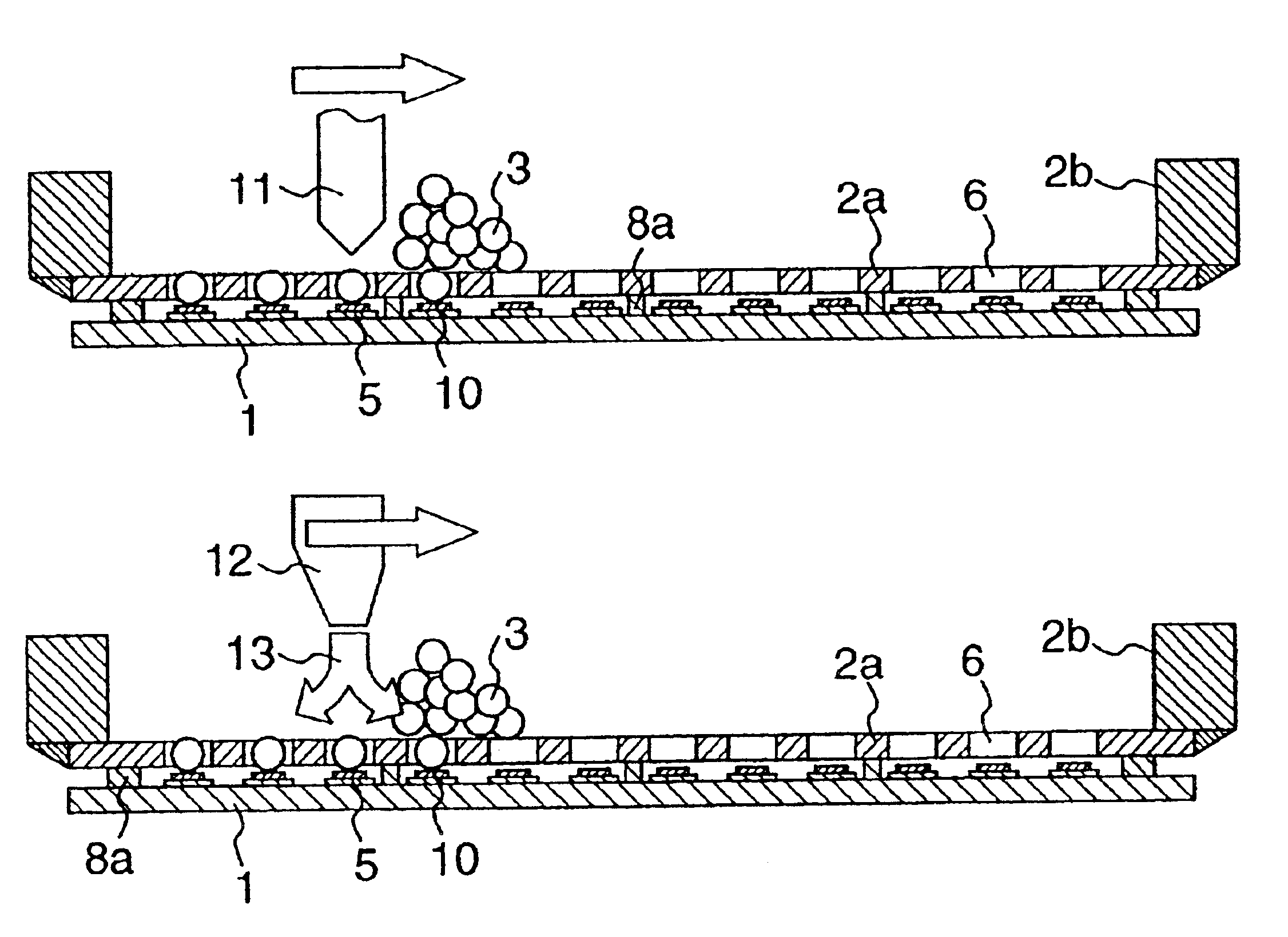
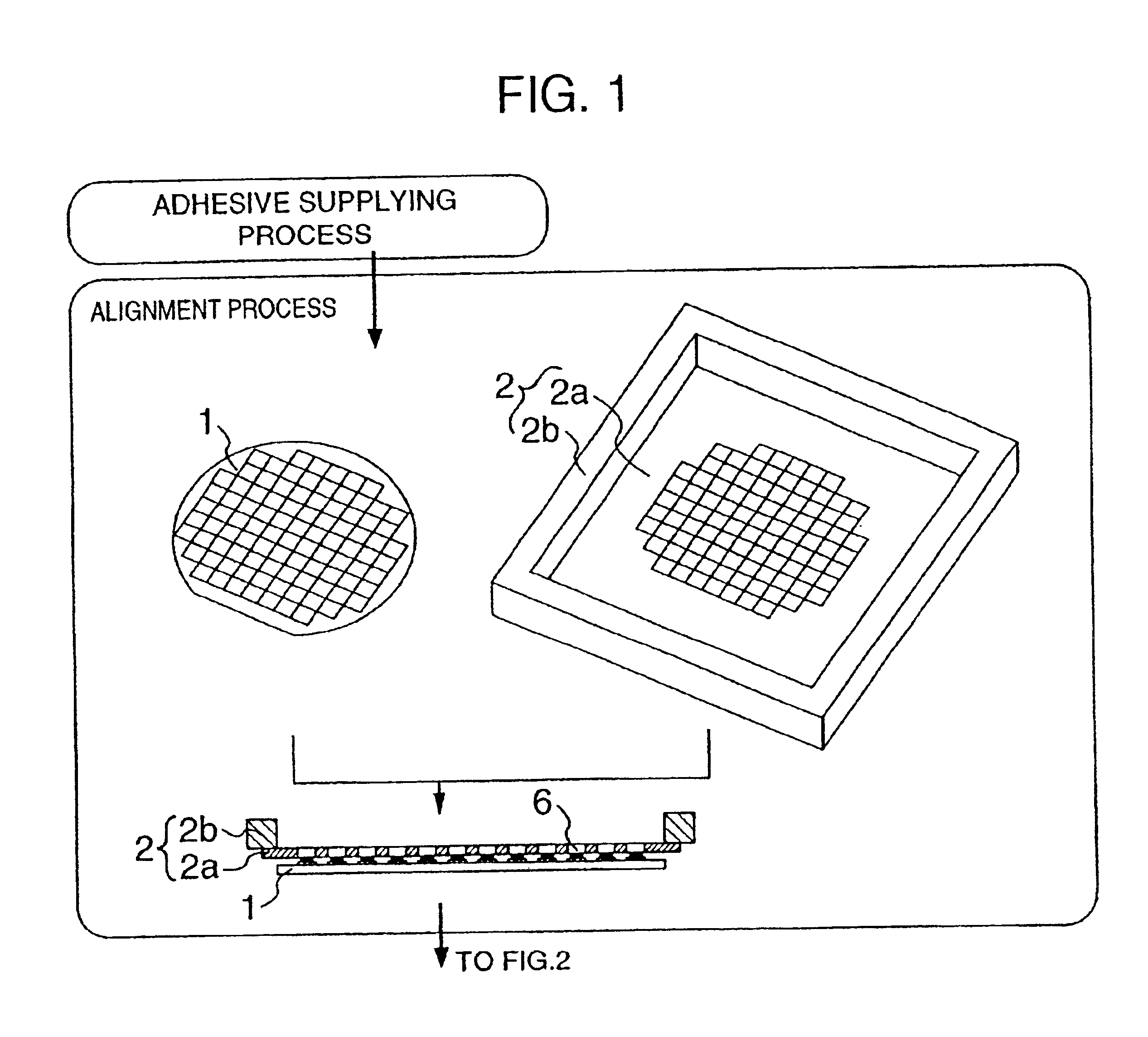
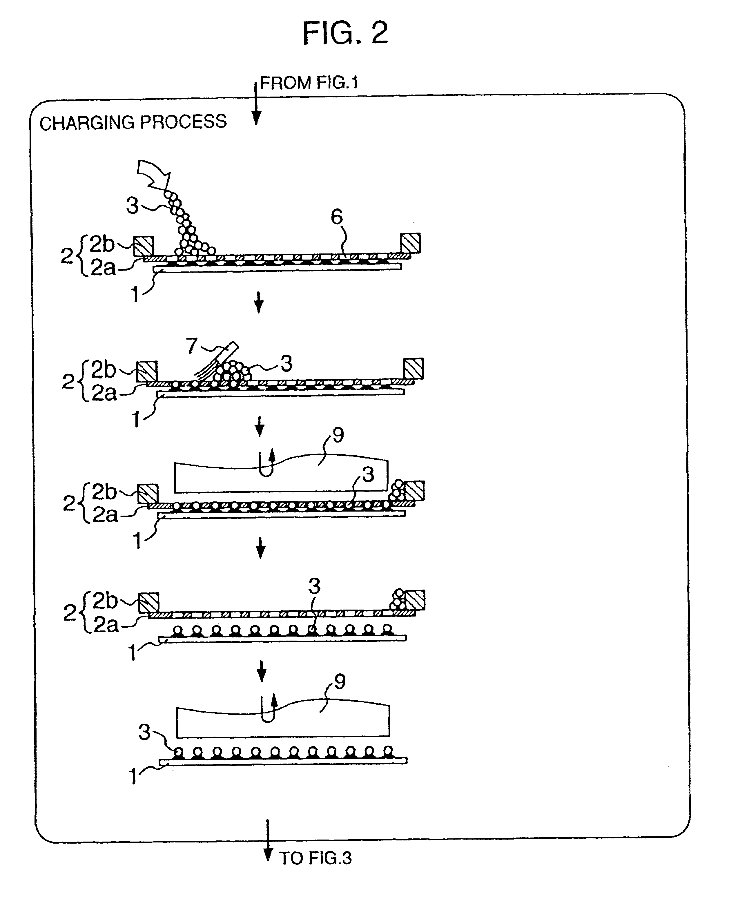
An embodiment of the invention will be described with reference to FIGS. 1 to 16. In those figures, like elements are identified by the same reference numerals, and will not be repeatedly described. FIGS. 1, 2 and 3 show a fundamental flow of the bump formation according to the invention. The bump formation flow according to the invention basically includes an alignment process, a ball charging process and a heating process as illustrated in FIGS. 1, 2 and 3. These processes will hereinafter be described in order, with reference to other figures, if necessary. Referring to FIGS. 1, 2 and 3, there are shown a semiconductor device 1 on which bumps are to be formed, a tool 2, conductive spheres 3, completed bumps 4, through-holes 6 of the tool 2 that will be described later, a brush 7, and a pressing tool 9. In addition, there are shown a stencil 2a of the tool 2, and a frame 2b of the tool 2. Although the semiconductor device 1 on which bumps can be formed according to the invention m...


PUM

PropertyMeasurementUnit
Thicknessaaaaaaaaaa
Diameteraaaaaaaaaa
Heightaaaaaaaaaa

Abstract

In the conventional bump forming method that can be applied to a semiconductor device in which a large number of bumps are required to be formed, there are various limitations on the material of which the bumps are made, due to enough cubic volume of bumps and to small scattering of the bump height. According to the invention, solder balls and a tool having a large number of through-holes are used, and under the condition that the through-holes of the tool are aligned with the pads of the semiconductor device, the solder balls are charged into the through-holes, pressed to be fixed on the pads, and then reflowed to form bumps.

Description

BACKGROUND OF THE INVENTIONThe present invention relates to a method of forming bumps as electrical, mechanical and thermal connections or contacts on a semiconductor device.There are many examples as to the method of forming bumps on a semiconductor device. For example, metal is deposited by plating to form bumps on the pads of a semiconductor device (plating method); a solder paste is printed on the pads of a semiconductor device, heated so that solder particles within the paste are melted, and thereafter solidified to form bumps on the pads (printing method); and one end of gold wire is bonded to a pad, and then the wire is cut so that the bonded part of wire is left as a bump (wire bonding method). In addition, as disclosed in U.S. Pat. No. 5,284,287, solder balls are sucked in the cavities of a pick-up tool by vacuum, placed on the pads of a semiconductor device and heated to melt, and solidified to form bumps (conventional type solder ball method).These conventional methods, h...

Claims


Application Information

Patent Timeline
IPC IPC(8): B23K3/06H01L21/68H01L21/60H01L21/02H01L21/67H05K3/34
CPCB23K3/0623H01L21/6835H01L24/11H05K3/3478H01L2224/11334H01L2224/11003H01L2224/13099H01L2924/01075H01L2924/01078H01L2924/01079H05K2203/0278H05K2203/0292H05K2203/041H05K2203/043H05K2203/0557H01L2924/01005H01L2924/01006H01L2924/014B23K2201/40H01L2224/45144H01L2224/05568H01L2224/05023H01L2224/05001H01L2924/00014B23K2101/40H01L2924/00H01L2224/05541H01L2224/05005H01L2224/05599H01L2224/05099
Inventor INOUE, KOSUKENISHIMURA, ASAOSUZUKI, TAKAMICHIFUJII, TERUMORISHIMA, MASAYUKINAKAJIMA, YASUYUKIOROKU, NORIYUKI
Owner RENESAS ELECTRONICS CORP
Why Eureka
Try Eureka