High-density illumination system

a high-density, illumination system technology, applied in the direction of lighting and heating apparatus, semiconductor devices of light sources, instruments, etc., can solve the problems of inconvenient use, insufficient illumination, and insufficient illumination, and achieve the effect of maintenance, and reducing the cost of operation

Active Publication Date: 2005-03-29
SNAPTRACK
View PDF2 Cites 689 Cited by
  • Summary
  • Abstract
  • Description
  • Claims
  • Application Information

AI Technical Summary

Benefits of technology

It is an additional object the invention to provide an improved system and method for making one or two-dimensional arrays of metallically reflecting bins having sloped or tapered sidewalls whose arrangement allows physical through-holes in the array defining both input and output apertures, the associated input aperture array spatially arranged so that each input aperture matches the size and shape of each LED chip in a corresponding array so that when brought together each LED chip fits simultaneously through each corresponding input aperture without mechanical interference blocking such a fit so that each chip thereby protrudes into each bin.
It is also an additional object of the invention to provide a compact means for efficiently converting un-polarized output light from a multi-layered LED light source array into substantially polarized output light using the metallically-reflecting nature of the reflecting bins involved and the metallically-reflecting nature of the LED's electrodes, in conjunction with elevated polarization converting films.

Problems solved by technology

Currently available illumination systems capable of achieving equivalent brightness uniformity (and lumen density) using only conventional optical elements, do so with at least 2 times fewer lumens per square millimeter, less efficiently (in terms of brightness), and in considerably thicker and less well-integrated packaging structures.
Currently available LED illumination systems use arrays of discretely packaged LED devices, or LED chips on interconnection planes disposed below conventional refractive optical elements (whose effective optical collection range is limited).
Using LEDs in place of short-arc discharge lamps, however, is not straightforward for several reasons.
Imagining the use of today's best high-power LEDs at light levels of 7000 to 9000 lumens seems quite difficult, given that best emission efficacies are only in the range of only 15-25 lumens per watt.
What's more, manufacturing economies keep typical LCD and DMD image apertures less than 1.2″ on the diagonal, and such devices cannot make effective use of light at angles above + / −12 degrees.
Even were such jumbo chips available, the challenge would still be to convert all its generated lumens to the + / −12-degrees needed in practical image projectors with high enough efficiency and spatial illumination uniformity.

Method used


Image

  • High-density illumination system
  • High-density illumination system
  • High-density illumination system

Examples


Embodiment Construction

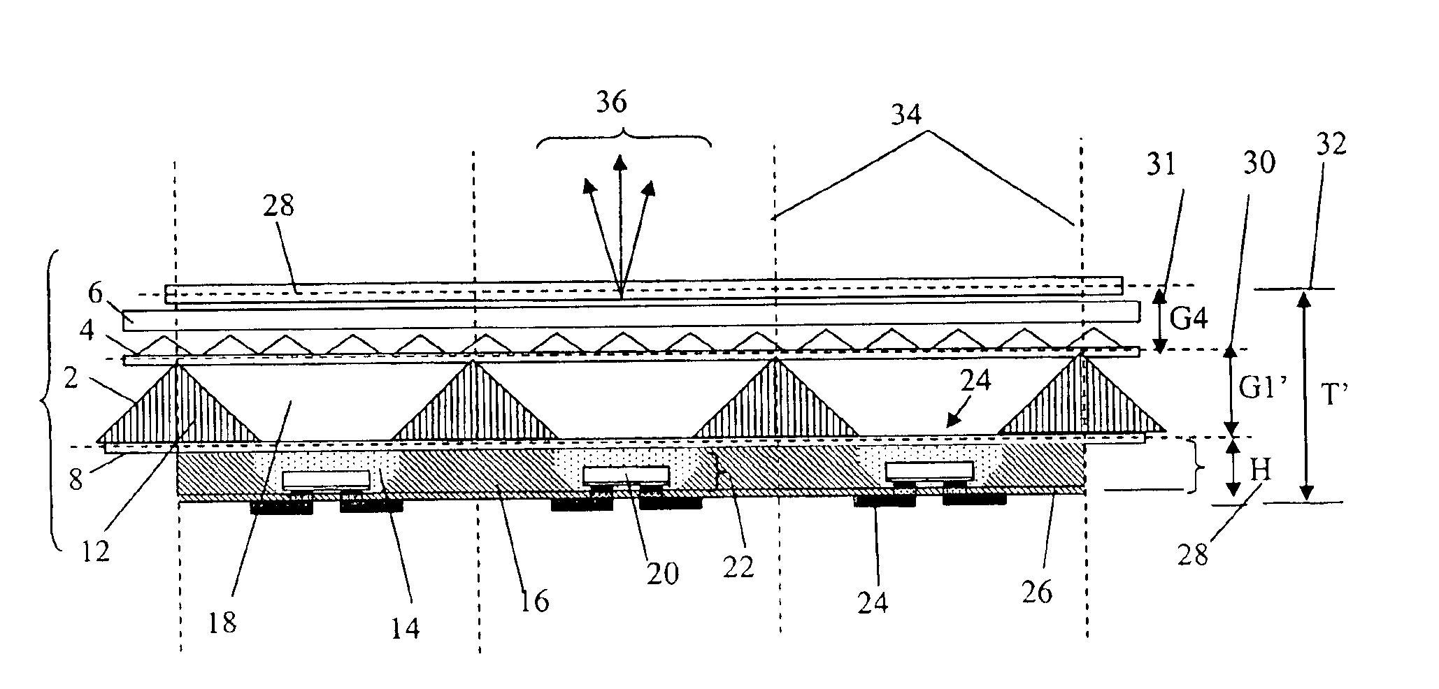
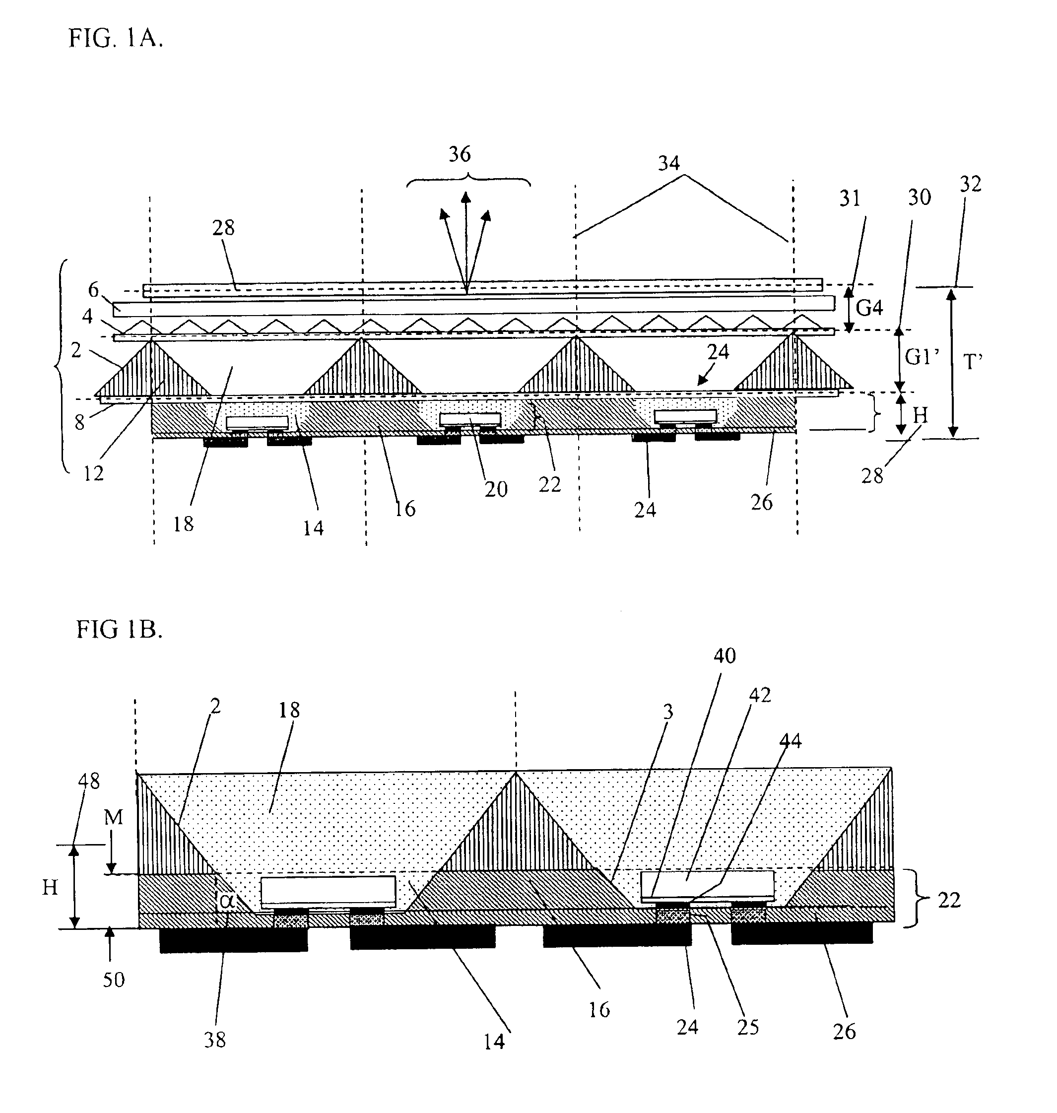
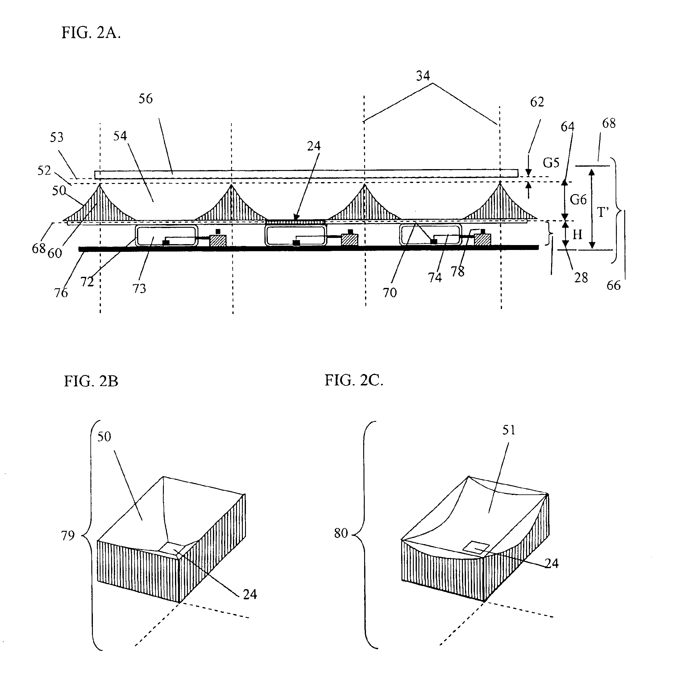
The present inventions relate to multi-layered packaging structures whose structural details maximize optical output from arrays of interconnected light emitting diodes (LEDs) over earlier multi-layered packaging structures. Specifically, the present inventions allow for the highest possible concentrations of output lumens per square millimeter of output aperture. This improvement leads to designs that allow earliest possible use of LED arrays as practical replacements for light bulbs in demanding applications such as video projection. This improvement also leads to related designs that use the minimum number of LEDs for the intended purpose.

Previous inventions, such as 10 in FIGS. 1A-B and 66 in FIG. 2A, have described the use of specially-shaped and sized reflecting bins surrounding each LED (or groups of LEDs) in the array with the bins arranged to work in conjunction with the design of certain reflective multi-layers placed just above them, such as for example prism sheets 4 and...


PUM

PropertyMeasurementUnit
depthaaaaaaaaaa
depthaaaaaaaaaa
depthaaaaaaaaaa

Abstract

A compact and efficient optical illumination system featuring planar multi-layered LED light source arrays concentrating their polarized or un-polarized output within a limited angular range. The optical system manipulates light emitted by a planar array of electrically-interconnected LED chips positioned within the input apertures of a corresponding array of shaped metallic reflecting bins using at least one of elevated prismatic films, polarization converting films, micro-lens arrays and external hemispherical or ellipsoidal reflecting elements. Practical applications of the LED array illumination systems include compact LCD or DMD video image projectors, as well as general lighting, automotive lighting, and LCD backlighting.

Description

BACKGROUND OF THE INVENTIONThe present invention, which is an expansion on inventions described in a previously filed application, entitled Uniform Illumination System filed on Dec. 14, 2001, Ser. No. 10 / 31980C, and which is incorporated by reference herein, is concerned generally with a thin and compact multi-layered optical system and method for generating well-organized output illumination from a one or two-dimensional array of discrete light emitting diodes (LEDs), the output light spread uniformly over the system's aperture while emanating from a uniquely multi-layered system comprised of reflecting bins and elevated light directing films. The present invention focuses centrally on the beneficial interactions between the geometric parameters of a thin array of metallically-reflecting bins, each having four tapered sidewalls meeting at an input aperture containing an LED, and the geometric parameters of orthogonally oriented prism sheets (and / or polarization converting sheets) p...

Claims


Application Information

Patent Timeline
Patent Type & Authority Patents(United States)
IPC IPC(8): F21V8/00F21K99/00G02B5/04G02B5/10G02B6/00G02B17/00G02F1/13357H01L33/58H01L33/60
CPCG02B5/10G02B6/0028G02B6/0036G02B6/0038G02B6/0053G02B6/0055G02B6/0073G02B17/002G02F1/133603G02F1/133605H04N9/315G02B5/045F21K9/00H01L2224/13H01L33/58H01L33/60H01L2933/0091Y10S362/80H01L2924/12044H01L2224/45144H01L2224/05573H01L2224/05568H01L2924/00014F21K9/68H01L2924/00H01L2224/05599
Inventor HOLMAN, ROBERT L.COX, ARTHUR
Owner SNAPTRACK
Why Eureka
Try Eureka