

Water-stable photoluminescent semiconductor nanocrystal complexes and method of making same
a nanocrystal complex, photoluminescent technology, applied in the direction of cellulosic plastic layered products, natural mineral layered products, other chemical processes, etc., can solve the problems of reducing limiting the number of tests that can be performed in a single assay, and lack of tight binding of hydrophilic coatings to nanocrystal surfaces. , to achieve the effect of reducing oxygen ability and preventing
- Summary
- Abstract
- Description
- Claims
- Application Information
AI Technical Summary
Benefits of technology
Problems solved by technology
Method used
Image

Examples
example 1
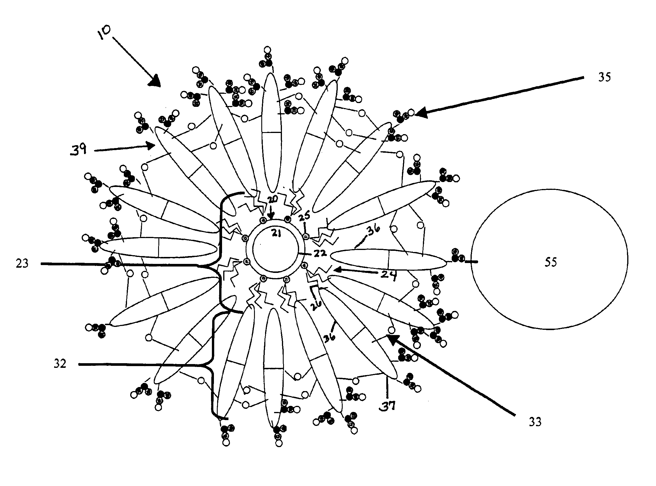
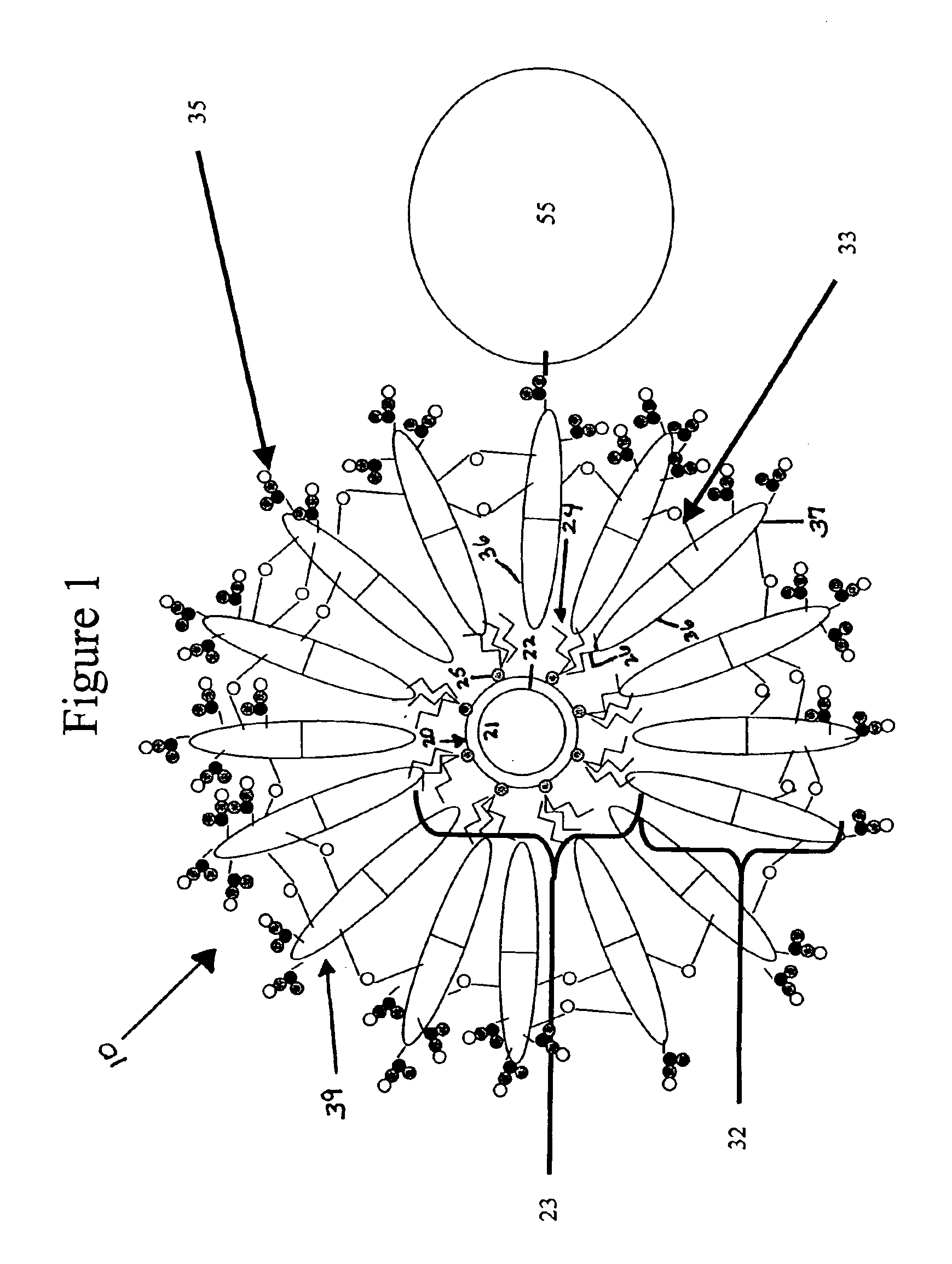
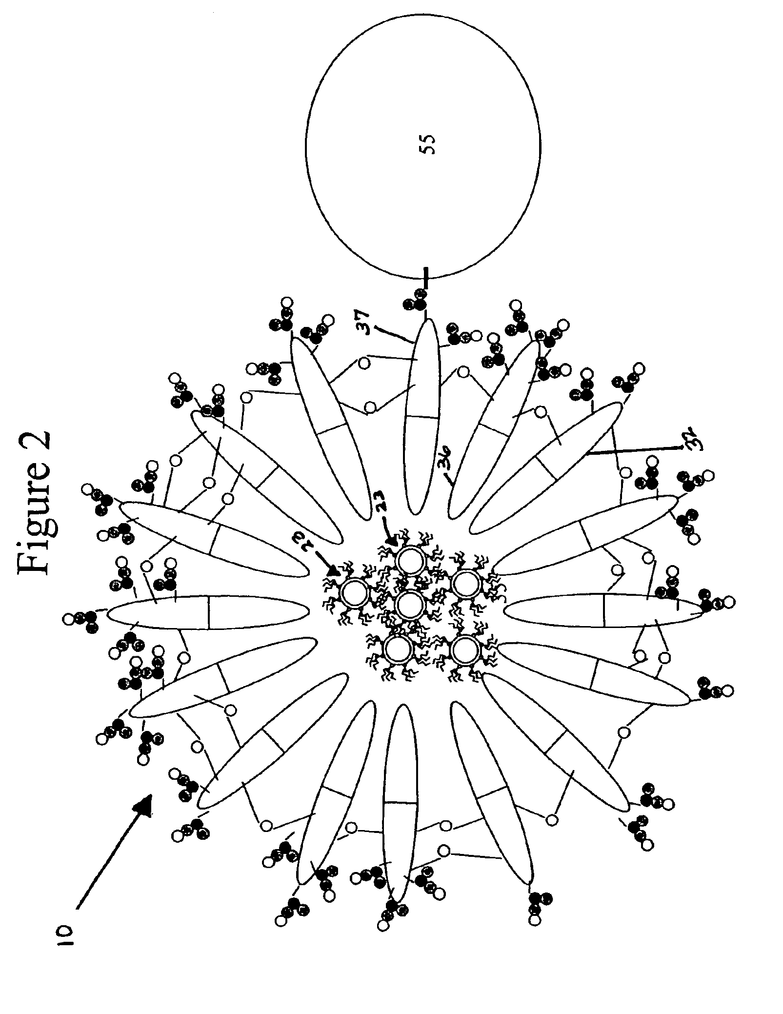
[0029]The following example discloses a method of assembling diblock polymers 32 having hydrophilic ends 37 comprising carboxy groups around a semiconductor nanocrystal 20 to form a semiconductor nanocrystal having a diblock polymer coating 39 assembled therearound (i.e. a semiconductor nanocrystal-loaded micelle).
[0030]Semiconductor nanocrystals in toluene (2 ml) or hexane solution (˜5 nmol / ml) were precipitated by the addition of methanol (8 ml) and centrifugation. The nanocrystals were further precipitated by drawing off the supernatant, resuspending the nanocrystals in pure hexane and repeating the precipitation step. The purification process was repeated for three times and the resulted precipitates were reconstituted in chloroform (1 ml).
[0031]A diblock polymer solution was prepared by dissolving poly(butadiene (1,4 addition)-b-acrylic acid) or poly(styrene-b-acrylic acid) (50 mg) in a mixture of chloroform (5 ml) and methanol (1:1). The solution was titrated by the organic ba...
example 2
[0032]The present example discloses a method of cross-linking adjacent ones of the diblock polymers 32 to form a semiconductor nanocrystal complex 10.
[0033]To further stabilized nanocrystals in aqueous solution, the polymer coating assembled around the nanocrystal surface as described in Example 1 was cross-linked using diamine molecules as linkers. Phosphate buffer (0.5M, 0.4 ml) was added to the nanocrystal-loaded micelle solution (5 ml) obtained in example 1 to adjust pH of the solution to 6.5. EDC (1-thyl-3-(3(-dimethylamionpropyl) carbodiimide hydrochloride) (10 mg) and sulfo-NHS (N-hydroxysulfosuccinimide sodium salts) (20 mg) were added to the solution to activate the carboxylic groups of the polymer assembled around the semiconductor nanocrystal surface. After 30 minutes, a solution (0.1 ml) of Bis (2,2′-(ethylenedioxy)bis(ethylamine))(20 mg / ml) was added gradually into the above solution, and the pH was raised to 8.5 immediately using NaOH solution (1N). The reaction soluti...
example 3
[0036]The present example discloses a method of conjugating a tertiary molecule (streptavidin) 55 to the semiconductor nanocrystal complex 10.
[0037]Phosphate buffer (0.5M, 0.2 ml, pH 6.5) was added to the nanocrystal-loaded micelle solution (2 ml) from Example 1. To activate the carboxylate group, EDC (10 mg) and sulfo-NHS (20 mg) were added to the solution. The solution was stirred (20 minutes), then streptavidin (4 mg) was added to this solution, and the pH of the solution was raised to 8.5 immediately using NaOH (1N) stock solution. The reaction was allowed to proceed for 2 hours, then purified by G-25 column to remove the unreacted chemicals and byproducts formed during the reaction.
[0038]FIG. 6 illustrates an image of a hybridization assay, captured by a fluorescent microscopy imager operably linked to a CCD camera, where semiconductor nanocrystal complexes are coupled to streptavidin proteins(s). Under ultraviolet illumination, the semiconductor nanocrystal complexes emit ligh...
PUM
| Property | Measurement | Unit |
|---|---|---|
| Hydrophilicity | aaaaa | aaaaa |
| Hydrophobicity | aaaaa | aaaaa |
| Semiconductor properties | aaaaa | aaaaa |
Abstract
Description
Claims
Application Information