Device transferring method, and device arraying method and image display unit fabricating method using the same

a technology of image display unit and transfer method, which is applied in the manufacture of electrode systems, electric discharge tubes/lamps, instruments, etc., can solve the problems of difficult to heat only the desired parts, positional deviation and peeling of other parts, and complicated work, etc., to achieve efficient and accurate transfer of devices

Inactive Publication Date: 2005-03-29
XIAMEN SANAN OPTOELECTRONICS CO LTD
View PDF68 Cites 159 Cited by
  • Summary
  • Abstract
  • Description
  • Claims
  • Application Information

AI Technical Summary

Benefits of technology

The present invention provides a device transferring method capable of transferring with certainty only those devices to be transferred of devices on a substrate, thereby efficiently and accurately transferring the devices, and provides a device arraying method and an image display unit fabricating method using the device transferring method.
With this image display unit fabricating method, the light emitting devices are arrayed in a matrix by making use of the above-described device transferring method and the device arraying method, to form an image display portion. Accordingly, since portions, near the devices to be transferred, of the adhesive layer can be efficiently, certainly heated, it is possible to efficiently, certainly perform the transfer of the devices. This makes it is possible to efficiently re-array the light emitting devices, which have been formed on the first substrate densely, that is, with a high degree of integration, on the second substrate in such a manner as to be spaced from each other with an enlarged pitch, and hence to significantly improve the productivity.

Problems solved by technology

In particular, for an image display unit such as an LCD or PDP, device isolation cannot be performed, so that in general, at the beginning of the fabrication process, devices are formed in such a manner as to be spaced from each other with a pitch equivalent to a pixel pitch of the image display unit.
In the case of using such a method, however, there arises a problem that since the electronic parts must be placed one by one, the work becomes complicated, and since the entire substrate is heated, there occurs the positional deviation and peeling of other parts.
Parts to be transferred and parts not to be transferred can be selectively transferred by using the above transfer method; however, according to the existing technique, it is difficult to heat only the desired parts, and therefore, this method has been not put into practical use.
Accordingly, in general, it is required to coat portions, at which parts are to be placed, of the substrate with a resin, and therefore, it fails to solve the above-described problem associated with the complicated work.
Similarly, there may be considered a method of picking up electronic parts once from a supply source by using an attracting head and placing them on a substrate; however, in this method, if the entire substrate is heated in the case of fixedly transferring the electronic parts from the attracting head to the substrate, there may occur an inconvenience that other parts having been already fixed to the substrate be peeled therefrom.
In the case of performing overall heating by laser irradiation, if either of a thermoplastic resin and each part has a low light absorptivity against laser beams, there occurs a problem that the thermoplastic resin is not heated to a desired temperature.
This method, however, has problems that since a plurality of steps of picking up each device by the attracting head, moving the attracting head, and placing the device to the substrate are required to transfer the devices, the transfer process becomes complicated, and since a plurality of kinds of equipment are required to be provided, the cost is raised, and that since the devices must be picked up one by one for mounting the devices, the mounting work becomes very complicated, and it takes much time to transfer the devices.
If it is intended to improve the working efficiency of the mounting machine for shortening the time required to mount the devices, there occurs another problem that the accuracy of arraying of the device at the time of mounting the devices is degraded.
Additionally, in the case of using the existing mounting machine, the positioning accuracy at the time of arraying devices has a limitation to about 10 μm, and therefore, it is difficult to further enhance the positioning accuracy by the existing positioning method.

Method used


Image

  • Device transferring method, and device arraying method and image display unit fabricating method using the same
  • Device transferring method, and device arraying method and image display unit fabricating method using the same
  • Device transferring method, and device arraying method and image display unit fabricating method using the same

Examples


second embodiment

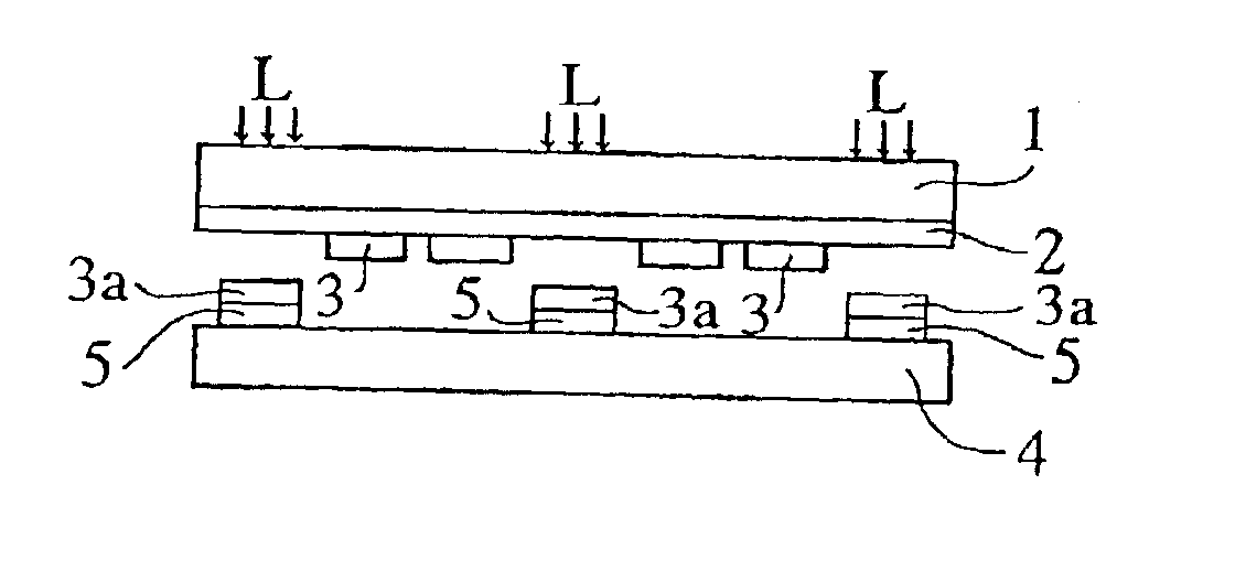
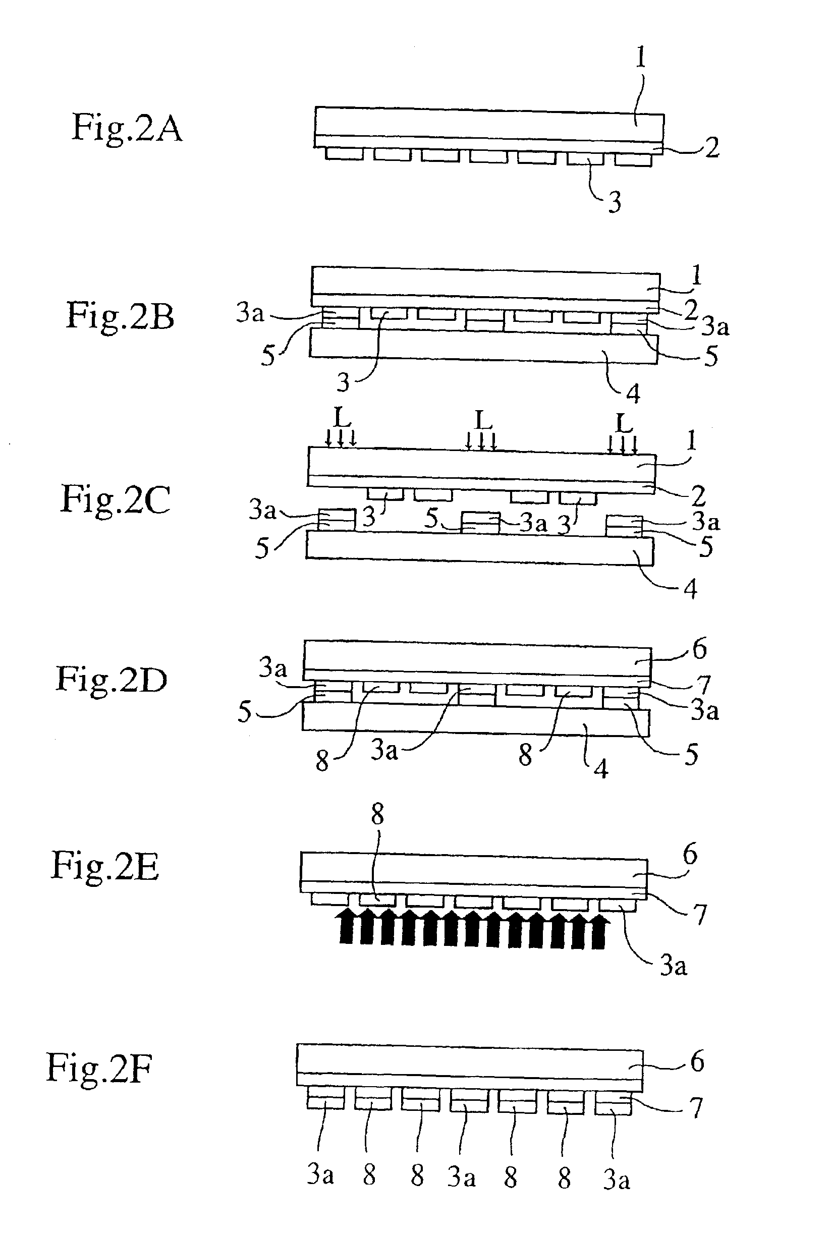
In the above-described method of arraying light emitting diodes, since the device transferring method is used, that is, since the light absorbing material 56a for increasing a light absorptivity of the adhesive layer 56 against the laser beams 73 is contained in the adhesive layer 56, it is possible to efficiently, selectively heat the portion, corresponding to each light emitting diode 42 to be transferred, of the adhesive layer 56, and hence to efficiently array the light emitting diodes 42.

The presence of the light absorbing material 56a for increasing a light absorptivity of the adhesive layer 56 against the laser beams 73 has another advantage that since the laser beams 73 are absorbed by the light absorbing material 56a and therefore the laser beams 73 do not reach the light emitting diode 42, with a result that the light emitting diode 42 is prevented from being damaged by the laser beams 73. As a result, it is possible to array the light emitting diodes 42 without damaging ...

third embodiment

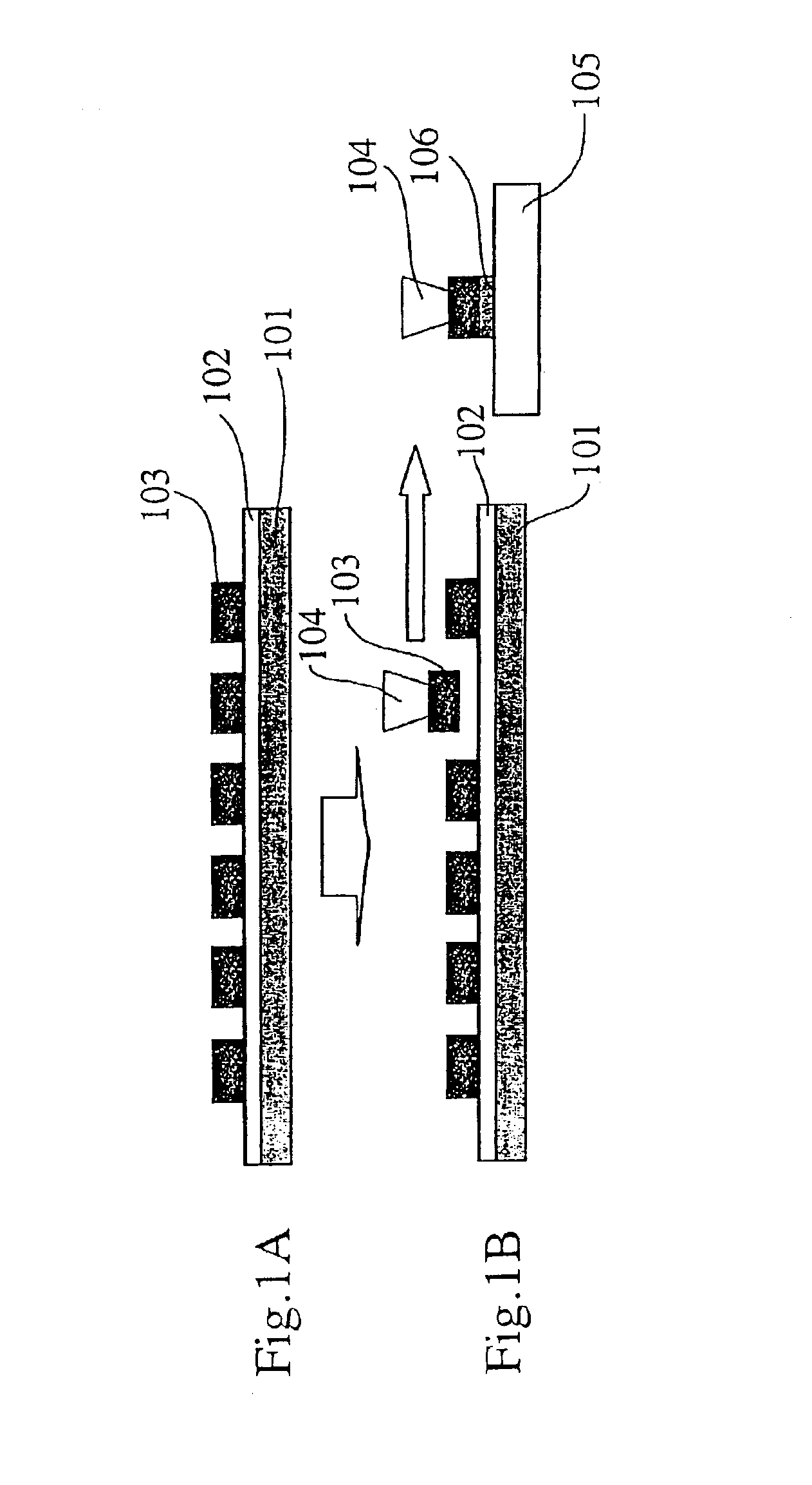
In the device transferring method described above, since the peeling of the devices 3 from the base substrate 1 and the adhesive bonding of the devices 3 to the transfer substrate 83 can be performed only by the heating process, it is possible to eliminate the need of providing an attracting head and an ultraviolet irradiation apparatus, which has been required in the case of using an ultraviolet reactive type material, and hence to transfer the devices 3 with a simple configuration. Since the transfer process is simple, the positioning of the devices 3 can be easily, certainly performed, so that it is possible to accurately transfer the devices without occurrence of any positional deviation in transferred devices. Further, by positioning a reference one of the devices 3 to be transferred at a specific position, the other devices to be transferred are collectively positioned at specific positions, it is possible to accurately transfer the devices without occurrence of any deviation...


PUM

PropertyMeasurementUnit
sizeaaaaaaaaaa
sizeaaaaaaaaaa
sizeaaaaaaaaaa

Abstract

A method of selectively transferring devices arrayed on a first substrate to a second substrate on which an adhesive resin layer is previously formed is provided. The method includes steps of selectively heating the adhesive resin layer on the second substrate by laser irradiation from the back surface side of the second substrate, and curing the selectively heated portions of the adhesive resin layer, thereby adhesively bonding those to be transferred of the devices to the second substrate. At this time, portions, corresponding to the devices, of the adhesive layer are heated directly or indirectly via the devices or wiring portions by laser irradiation from the back surface side of the substrate. The heated portions of the adhesive resin layer selectively exhibit the adhesive forces. The heated portions of the adhesive layer are then cured, so that only the devices to be transferred are selectively transferred to the second substrate. As a result, only the devices to be transferred can be done so with certainty, efficiency, and accuracy without exerting adverse effect on other parts.

Description

RELATED APPLICATION DATAThe present application claims priority to Japanese Patent Application Nos. P2001-112401 filed on Apr. 11, 2001; P2001-169857 filed on Jun. 5, 2001; P2001-194890 filed on Jun. 27, 2001; herein incorporated by reference.BACKGROUND OF THE INVENTIONThe present invention relates to a device transferring method of transferring devices such as semiconductor light emitting devices, and a device arraying method and an image display unit fabricating method for transferring finely formed devices to a wider region by using the device transferring method.At present, an array of a number of fine devices, electronic parts, electronic devices, or electronic parts formed by burying the above devices or parts in an insulator such as a plastic material are being extensively used for electronic equipment.The assembly of an image display unit by arraying light emitting devices in a matrix is performed in two manners. For a liquid crystal display (LCD) or a plasma display panel (...

Claims


Application Information

Patent Timeline
Patent Type & Authority Patents(United States)
IPC IPC(8): H01L25/075B44C1/00B44C1/165H01L21/00H01L21/336H01L21/50H01L21/60H01L21/68
CPCH01L21/6835H01L24/82H01L24/18H01L2924/12041H01L25/0753H01L33/0079H01L33/20H01L2221/68318H01L2221/68354H01L2221/68359H01L2221/68368H01L2224/18H01L2224/82039H01L2924/01012H01L2924/01013H01L2924/01015H01L2924/0102H01L2924/01029H01L2924/01039H01L2924/01046H01L2924/01052H01L2924/01058H01L2924/01075H01L2924/01078H01L2924/01079H01L2924/3025H01L2924/01005H01L2924/01006H01L2924/01024H01L2924/01033H01L2924/014H01L21/568H01L24/24H01L2224/04105H01L2224/32225H01L2224/73267H01L2224/92244H01L2924/12042H01L33/0093H01L2924/00G02F1/136
Inventor HAYASHI, KUNIHIKOYANAGISAWA, YOSHIYUKIIWAFUCHI, TOSHIAKIOHBA, HISASHI
Owner XIAMEN SANAN OPTOELECTRONICS CO LTD
Why Eureka
Try Eureka