Flex-based IC package construction employing a balanced lamination

a balanced lamination and ic technology, applied in the direction of printed circuit non-printed electric components association, semiconductor/solid-state device details, etching metal masks, etc., can solve the problem of difficult to cost-effectively drill the rigid pcb to support the c4 pitch needed for most interposer designs geared for high bandwidth, and reduce the tendency of the assembly to warp. , the effect of thin metal stiffeners

Inactive Publication Date: 2005-04-05
IBM CORP
View PDF39 Cites 78 Cited by
  • Summary
  • Abstract
  • Description
  • Claims
  • Application Information

AI Technical Summary

Benefits of technology

It is another object of the present invention to provide a laminated flex circuit assembly that is capable for providing a very short z-dimension interconnection between opposed integrated circuit chips. It is another object of the present invention to provide a laminated flex circuit assembly that requires thinner metal stiffeners.
It is another object of the present invention to provide a laminated circuit assembly that permits close spacing of the chip edge to the border of the chip window.
It

Problems solved by technology

As a result, numerous power planes must be employed in the design to facilitate efficient power distribution, which results in a relatively thick interposer.
However, cost and availability of the glass ceramic construction make it less desirable for many high volume, low cost markets.
However, it is difficult to cost-effectively drill the rigid PCB to support the C4 pitch nece

Method used


Image

  • Flex-based IC package construction employing a balanced lamination
  • Flex-based IC package construction employing a balanced lamination
  • Flex-based IC package construction employing a balanced lamination

Examples


Embodiment Construction

The foregoing and other objects, features and advantages of the invention will be apparent from the following more particular description of a preferred embodiment of the invention, as illustrated in the accompanying drawings, wherein like reference numbers represent like parts.

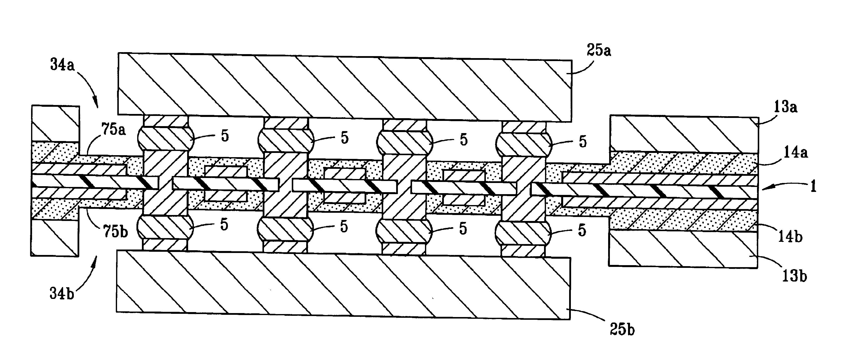
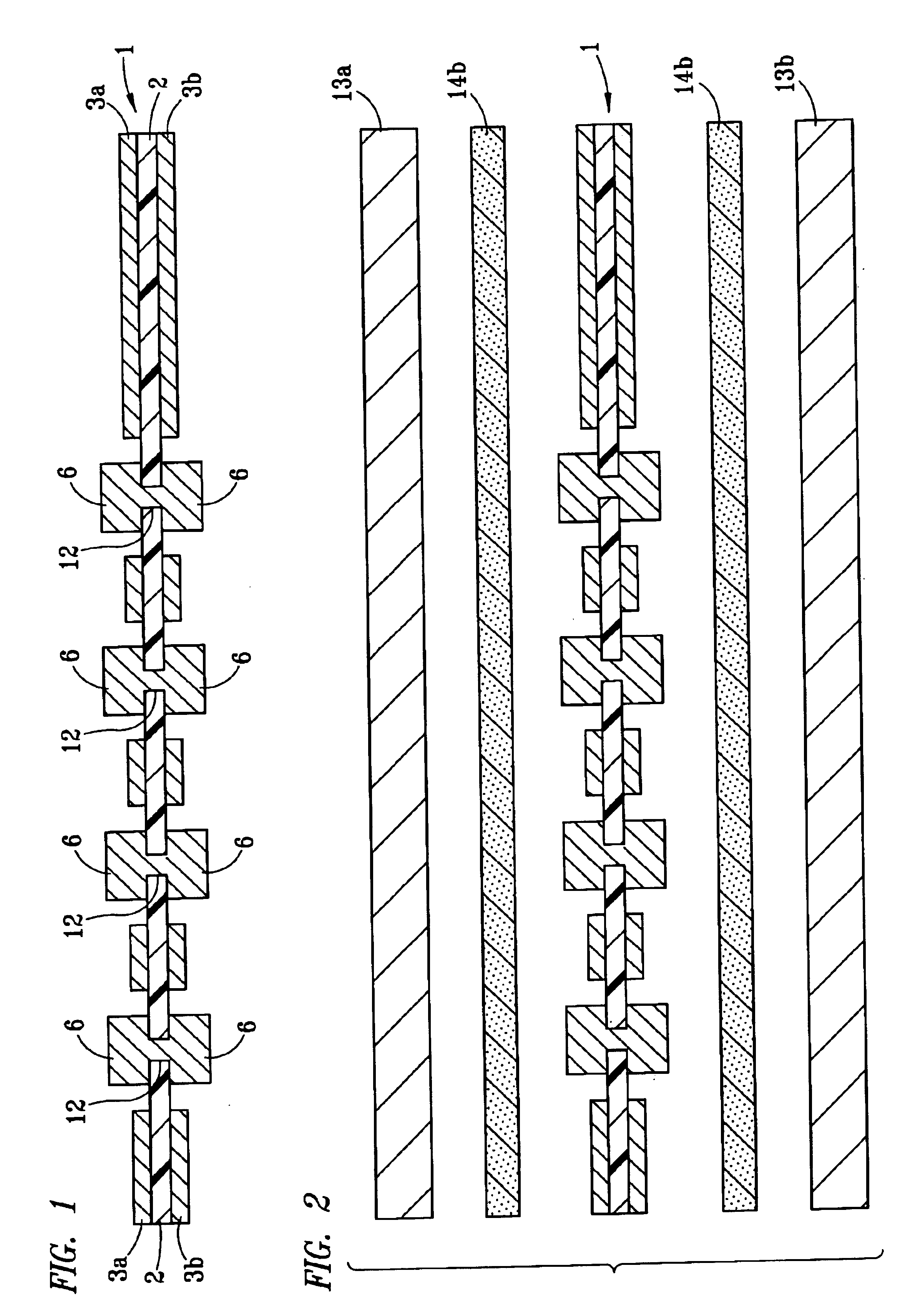
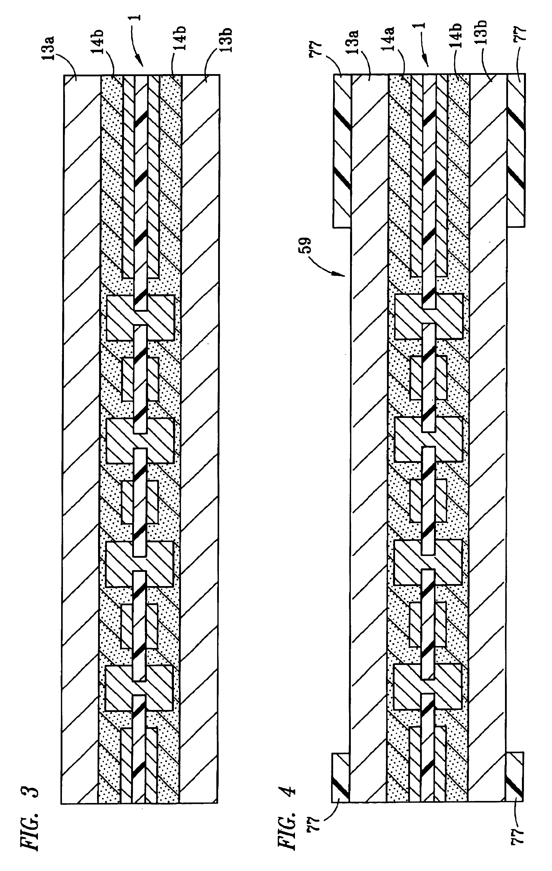
Turning now to the drawings in detail, and initially to FIG. 1 thereof, a 2ML bumped circuit layer 1, showing one representative raised bump 6 on each circuit layer, is depicted. The 2ML bumped circuit layer or assembly 1 has a medial insulating substrate 2, preferably polyimide, and is preferably though not necessarily of the type referred to as “flex” technology. The insulating substrate 2 is preferably thin, as thin as 25 microns or less, and has vias 12 defined in the z-dimension of the insulating substrate 2 which are preferably formed by using lasers, mechanical drilling or other means. It is to be understood that the bumps 6 are preferably generally symmetrical, so that the width of the bump 6 along th...


PUM


Abstract

The present invention provides for a balanced laminated integrated circuit package. The package includes a two metal layer bumped circuit, a first adhesive layer having a thickness on a first side of the bumped circuit, a first outer conductive layer having a thickness bonded to the first adhesive layer and a second adhesive layer having a thickness substantially equal to the thickness of the first adhesive layer on a second side of the bumped circuit. The invention also includes a second outer conductive layer bonded to the second adhesive layer, the second outer conductive layer having a thickness substantially equal to the thickness of the first outer conductive layer.

Description

BACKGROUND OF THE INVENTION1. Field of the InventionThis invention relates generally to the field of integrated circuit packaging.2. Description of the Related ArtIn the manufacture of integrated circuits, extremely fine circuits are photolithographically placed onto a chip, also called a die. The circuits on the chip terminate at conductive terminals on the face of the chip, which must be electrically connected to power and to other chips. For protection of the chip and ease of handling, these chips are bonded to a substrate and to electrical connections ultimately leading to conventional printed circuit boards. One attractive way of connecting the conductive terminals on a chip is where the terminals are distributed over the face of the chip and connected to a circuit substrate by conductive paste or solder balls in a pattern of “C4” connections.In some integrated circuit packaging applications, there are at least two integrated circuit chips having very high communication bandwid...

Claims


Application Information

Patent Timeline
IPC IPC(8): H01L25/065H05K1/02H05K3/00H05K3/40H05K3/46H05K1/11H05K1/18H01L23/32
CPCH01L25/0657H05K1/0218H05K2203/0554H01L2225/06517H01L2225/06541H01L2225/06579H01L2924/09701H01L2924/3011H05K1/113H05K1/189H05K3/002H05K3/4007H05K3/4652H05K2201/0367H05K2201/0715H05K2201/10674H01L2224/16225H01L2224/05568H01L2224/05573H01L2224/16235H01L2224/16238H01L2924/00014H01L2224/05599
Inventor HARVEY, PAUL MARLAN
Owner IBM CORP
Why Eureka
Try Eureka