

Method and apparatus for controlling data output frequency
- Summary
- Abstract
- Description
- Claims
- Application Information
AI Technical Summary
Benefits of technology
Problems solved by technology
Method used
Image

Examples
Embodiment Construction
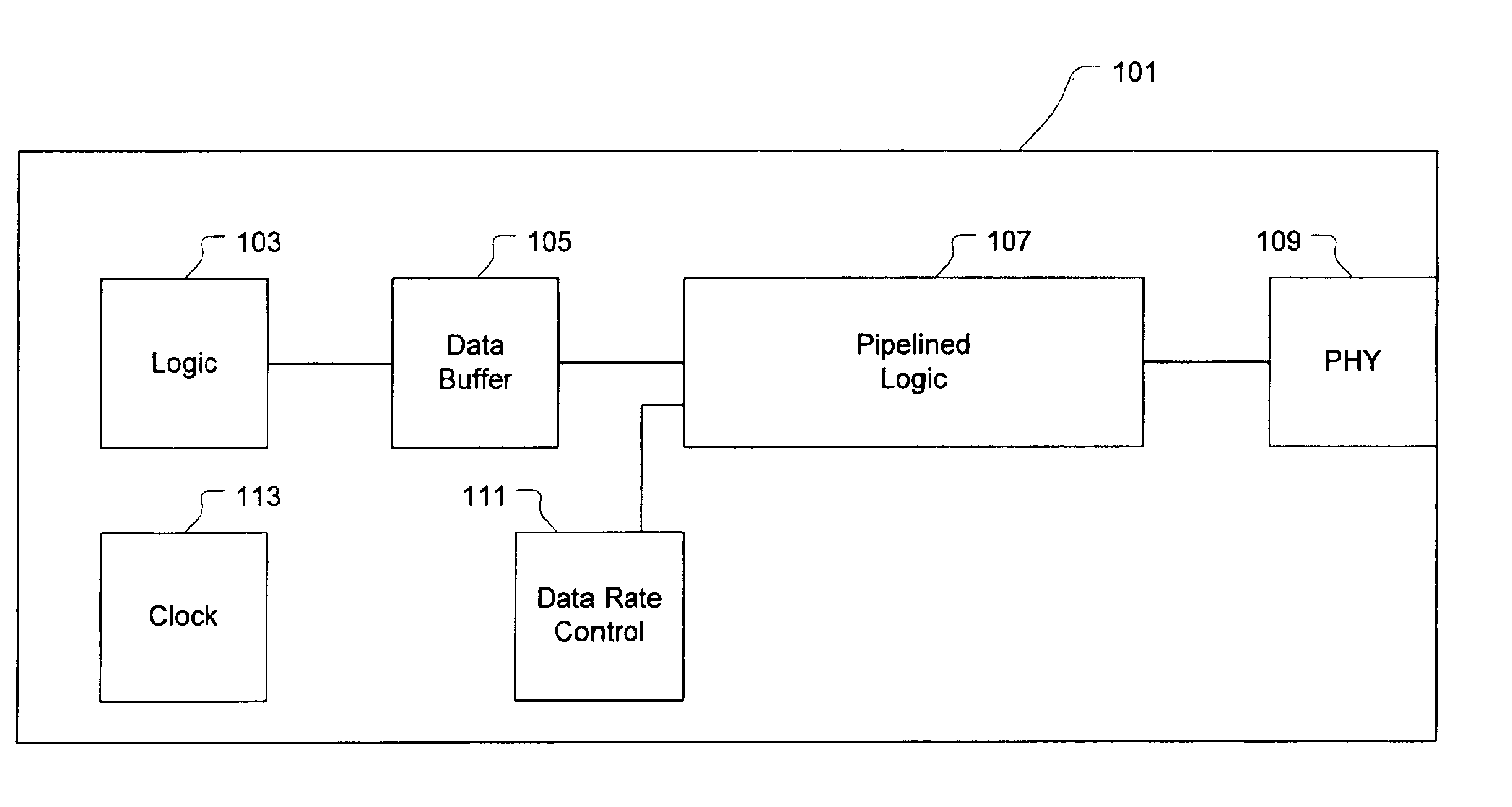
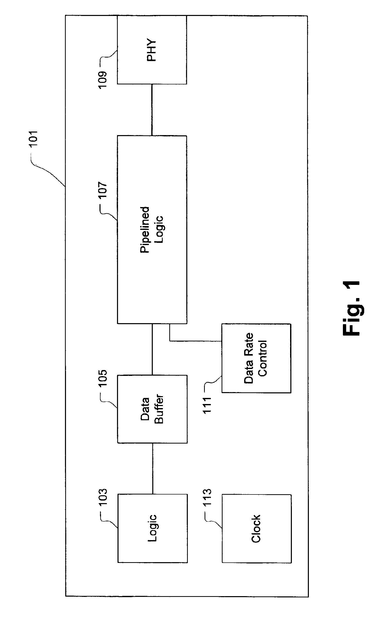
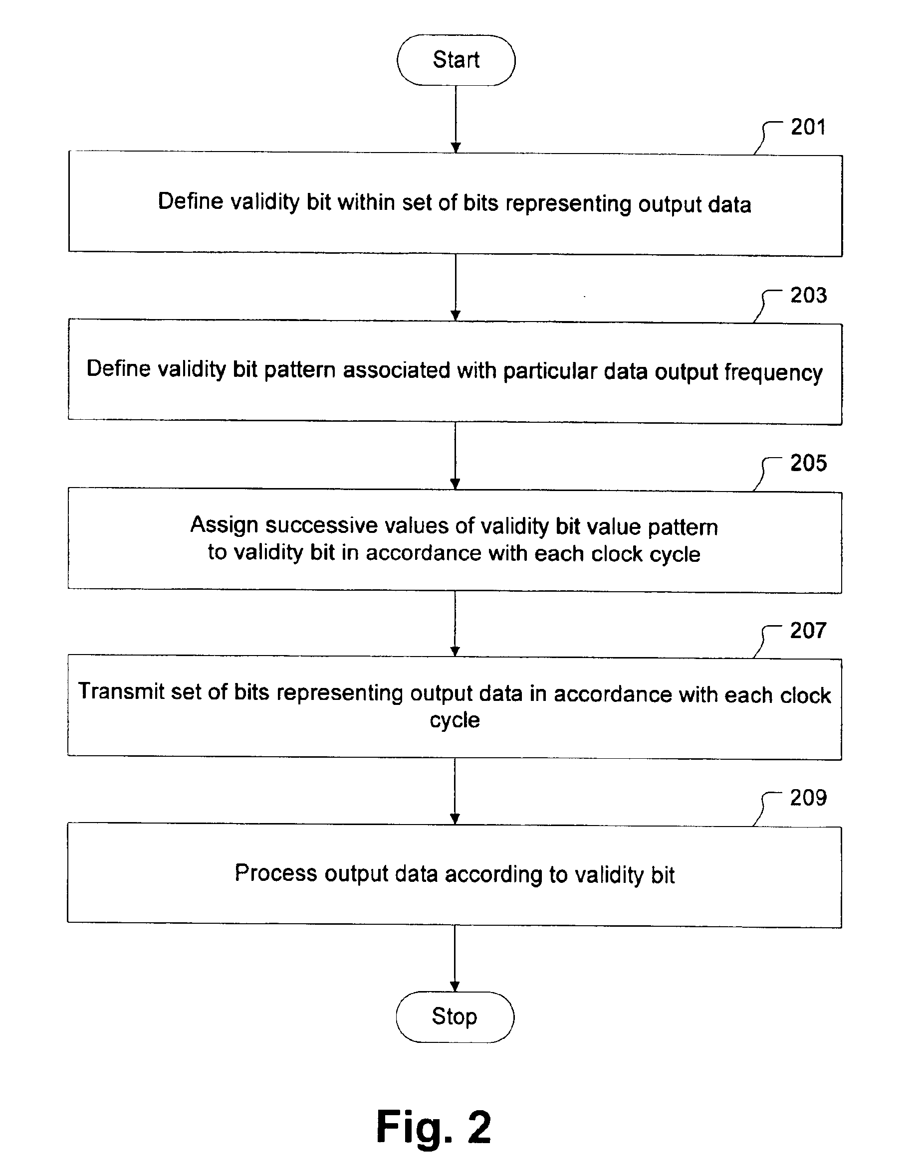
Broadly speaking, the present invention provides a method and corresponding apparatus for controlling a data output rate of an electronic device. More specifically, the method and corresponding apparatus of the present invention enables an equivalent data output rate to be obtained from each of an ASIC and an FPGA prototype of the ASIC while maintaining equivalent logic between the ASIC and the FPGA prototype. The present invention attaches a validity bit to each output data signal in accordance with each cycle of a clock signal, wherein the clock signal can be different between the ASIC and the FPGA prototype. The validity bit provides an indication as to whether the associated data signal should be processed normally as a valid data signal or discarded as an invalid data signal. Upon receipt of the data signal and associated validity bit at a transceiver, the data signal is processed according to a value of the validity bit. Thus, only valid output data signals are transmitted by ...
PUM
 Abstract
Description
Claims
Application Information