Polishing head of chemical mechanical polishing apparatus and polishing method using the same

a technology of mechanical polishing and polishing head, which is applied in the direction of grinding drives, lapping machines, manufacturing tools, etc., can solve the problems of high vacuum between the membrane and the wafer, wafer dropping or otherwise harmed, and the polishing head introduces limitations, etc., to achieve high polishing uniformity

Inactive Publication Date: 2005-04-19
SAMSUNG ELECTRONICS CO LTD
View PDF12 Cites 6 Cited by
  • Summary
  • Abstract
  • Description
  • Claims
  • Application Information

AI Technical Summary

Benefits of technology

[0010]It is an object of the present invention to provide an improved polishing apparatus and method for polishing a semiconductor wafer with high polishing uniformity.

Problems solved by technology

However, the vacuum between the membrane and the wafer often times leaks, such that during transfer, the wafer may be dropped or otherwise harmed.
However, such a polishing head introduces limitations that are shown in FIG. 1, which is a graph illustrating the resulting uneven surface of a wafer.
Portions A and B are relatively over-polished as compared to other portion of the wafer, thereby compromising the uniformity of polishing surface of the wafer.

Method used


Image

  • Polishing head of chemical mechanical polishing apparatus and polishing method using the same
  • Polishing head of chemical mechanical polishing apparatus and polishing method using the same
  • Polishing head of chemical mechanical polishing apparatus and polishing method using the same

Examples


first embodiment

[Modified First Embodiment]

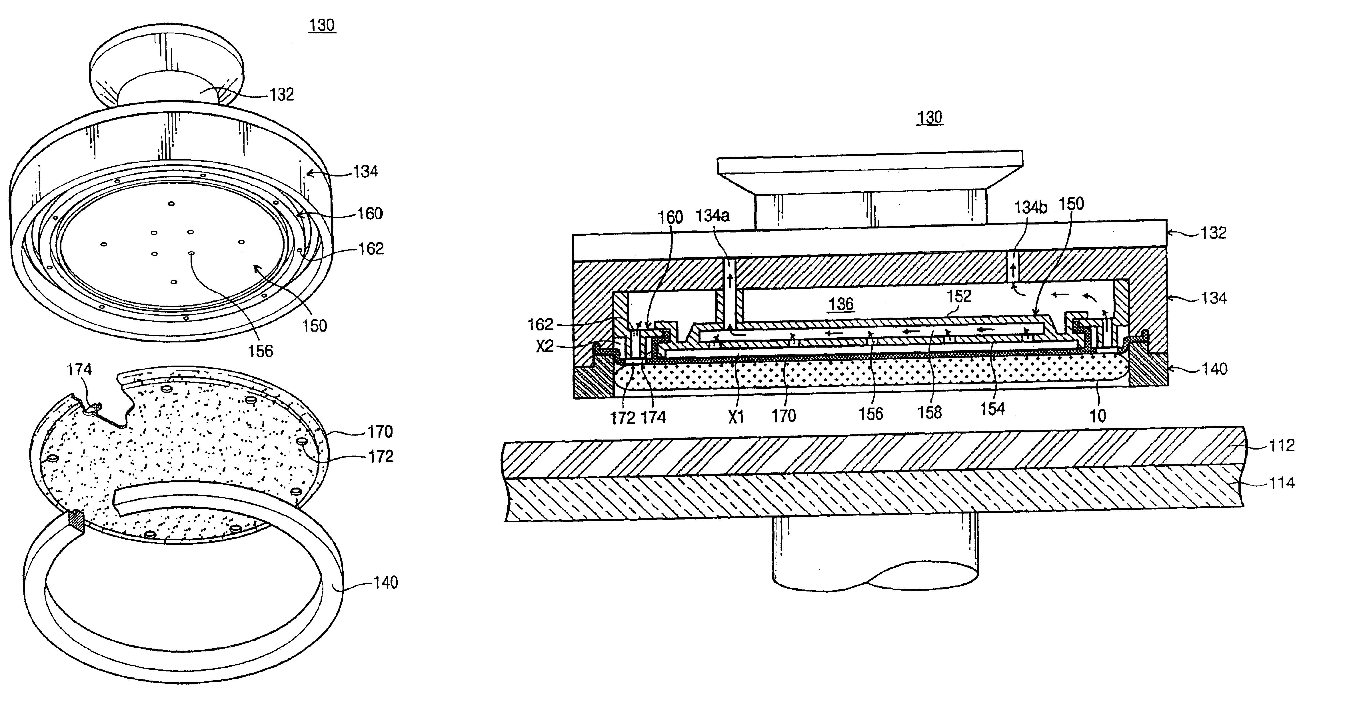
[0063]FIG. 7, FIG. 8, and FIG. 9 illustrate views of a polishing head 130a according to a modified first embodiment of the present invention. The polishing head 130a according to the modified first embodiment is nearly identical to a polishing head 130 according to the first embodiment with regard to characteristic structure and operation. The difference lies in that the modified polishing head 130a is divided into a plurality of regions X1 and X2 defined by the membrane, and a central region X3 where the membrane is not present. An independently controllable pressure can be provided to each of the regions X1, X2, X3.

[0064]The polishing head 130a of this embodiment includes a carrier 134, a center supporter 186, a middle supporter 188, a chucking ring 184, and a membrane 170a. The carrier 134 includes first, second and third gas gates 134a, 134b, and 134c. The center supporter 186 has a first chamber 187 which communicates with the first gas gate 134a, and...

second embodiment

[Second Embodiment]

[0072]FIG. 10 and FIG. 11 illustrate cross-sectional views of a polishing head according to a second embodiment of the present invention.

[0073]A polishing head 130b according the second embodiment is different from the polishing head 130 according to the first embodiment in that the chucking ring is moved up and down during chucking and polishing. For that reason, the polishing head 130b includes a manifold 132, a vessel-shaped carrier 134, a retaining ring 140, a center supporter 186, a middle supporter 188, a membrane 170b, a chucking ring 190, and a unit for moving the chucking ring.

[0074]The manifold 132 disperses four fluid providing channels to gas gates 134a, 134b, 134c, and 134d of the carrier 134. The carrier 134 includes the first, second, third and fourth gas gates 134a, 134b, 134c, and 134d. The center supporter 186 is installed in the carrier 134, and includes a first chamber 187 which communicates with the first gas gate 134a and a bottom side where ...


PUM

PropertyMeasurementUnit
vacuumaaaaaaaaaa
pressureaaaaaaaaaa
structureaaaaaaaaaa

Abstract

A chemical mechanical polishing (CMP) apparatus includes a polishing head that is composed of a carrier and a membrane, and is positioned on a polishing pad of a supporting part. The polishing head has a supporter installed at an internal center of the carrier, a chucking ring positioned between the carrier and the supporter, and means for moving the chucking ring up and down in a vertical direction. The supporter forms a sealed space together with the membrane, and the chucking ring chucks the wafer in vacuum.

Description

RELATED APPLICATIONS[0001]This application is a divisional application of U.S. patent application Ser. No. 10 / 107,612, filed Mar. 27, 2002 now U.S. Pat. No. 6,769,973, which is a continuation-in-part application of U.S. patent application Ser. No. 09 / 877,922, filed Jun. 7, 2001 now U.S. Pat. No. 6,652,362, the contents of which are incorporated herein by reference, in their entirety.[0002]This application relies for priority upon Korean Patent Application No. 2001-30365, filed on May 31, 2001, the contents of which are incorporated herein by reference, in their entirety.FIELD OF THE INVENTION[0003]The present invention generally relates to an apparatus and method for manufacturing a semiconductor wafer and, more particularly, to a chemical mechanical polishing (CMP) machine and related polishing method.BACKGROUND OF THE INVENTION[0004]As the elements incorporated into a semiconductor device are increasingly integrated, the structure of device wires such as gate lines and bit lines c...

Claims


Application Information

Patent Timeline
Patent Type & Authority Patents(United States)
IPC IPC(8): B24B37/04B24B41/06
CPCB24B41/061B24B37/30
Inventor BOO, JAE-PHILKIM, JONG-SOORYU, JUN-GYULEE, SANG-SEONLEE, SUN-WUNG
Owner SAMSUNG ELECTRONICS CO LTD
Why Eureka
Try Eureka