Memory devices having power supply routing for delay locked loops that counteracts power noise effects

a technology of delay lock loop and memory device, which is applied in the direction of digital storage, pulse automatic control, instruments, etc., can solve the problems of large power loss and nois

Inactive Publication Date: 2005-04-19
SAMSUNG ELECTRONICS CO LTD
View PDF4 Cites 12 Cited by
  • Summary
  • Abstract
  • Description
  • Claims
  • Application Information

AI Technical Summary

Benefits of technology

[0020]According to additional aspects of the present invention, a semiconductor memory device includes a data output path that receives an internal clock and data to be output and that synchronizes the data to the internal clock and outputs the synchronized data. The device further includes a delay locked loop (DLL) that receives an external clock and generates the internal clock therefrom, the DLL including a variable delay line which delays the internal clock with respect to the external clock in response to a delay control signal and DLL peripheral circuitry that generates the delay control signal from the external clock and a feedback clock that is derived from the internal clock and compensated for delay time of the data output path. The variable delay line receives dedicated power for the variable delay line, and the DLL peripheral circuitry receives dedicated power for the DLL peripheral circuitry.
[0021]In additional embodiments, a semiconductor memory device includes a data output path that receives an internal clock and data to be output and that synchronizes the data to the internal clock and outputs the synchronized data. A DLL receives an external clock and generates the internal clock therefrom, the DLL including a variable delay line that delays the internal clock with respect to the external clock in response to a delay control signal, and DLL peripheral circuitry that generates the delay control signal from the external clock and a feedback clock that is derived from the internal clock compensated for a delay time of the data output path. The device further includes a general-purpose power pad that receives general-purpose power to supply the general-purpose power to the data output path, a variable delay line power pad that receives dedicated power for variable delay line so as to supply the power to the variable delay line, and a peripheral circuitry power pad that receives dedicated power for peripheral circuitry so as to supply the power to the DLL peripheral circuitry.

Problems solved by technology

Typically, as the number of output pins connected to the output data path 200 increases, power dissipation is greatly increased, causing large power loss and noise.
This can cause jitter.

Method used


Image

  • Memory devices having power supply routing for delay locked loops that counteracts power noise effects
  • Memory devices having power supply routing for delay locked loops that counteracts power noise effects
  • Memory devices having power supply routing for delay locked loops that counteracts power noise effects

Examples


Embodiment Construction

[0029]The present invention now will be described more fully with reference to the accompanying drawings, in which embodiments of the invention are shown. This invention may, however, be embodied in many different forms and should not be construed as being limited to the embodiments set forth herein; rather, these embodiments are provided so that this disclosure will be thorough and complete, and will fully convey the concept of the invention to those skilled in the art. In the drawings, when an element is referred to as being “connected” or “coupled” to another element, it can be directly connected or coupled to the other element or intervening elements may be present. In contrast, when an element is referred to as being “directly connected” or “directly coupled” to another element, there are no intervening elements present. Like reference numerals refer to like elements throughout.

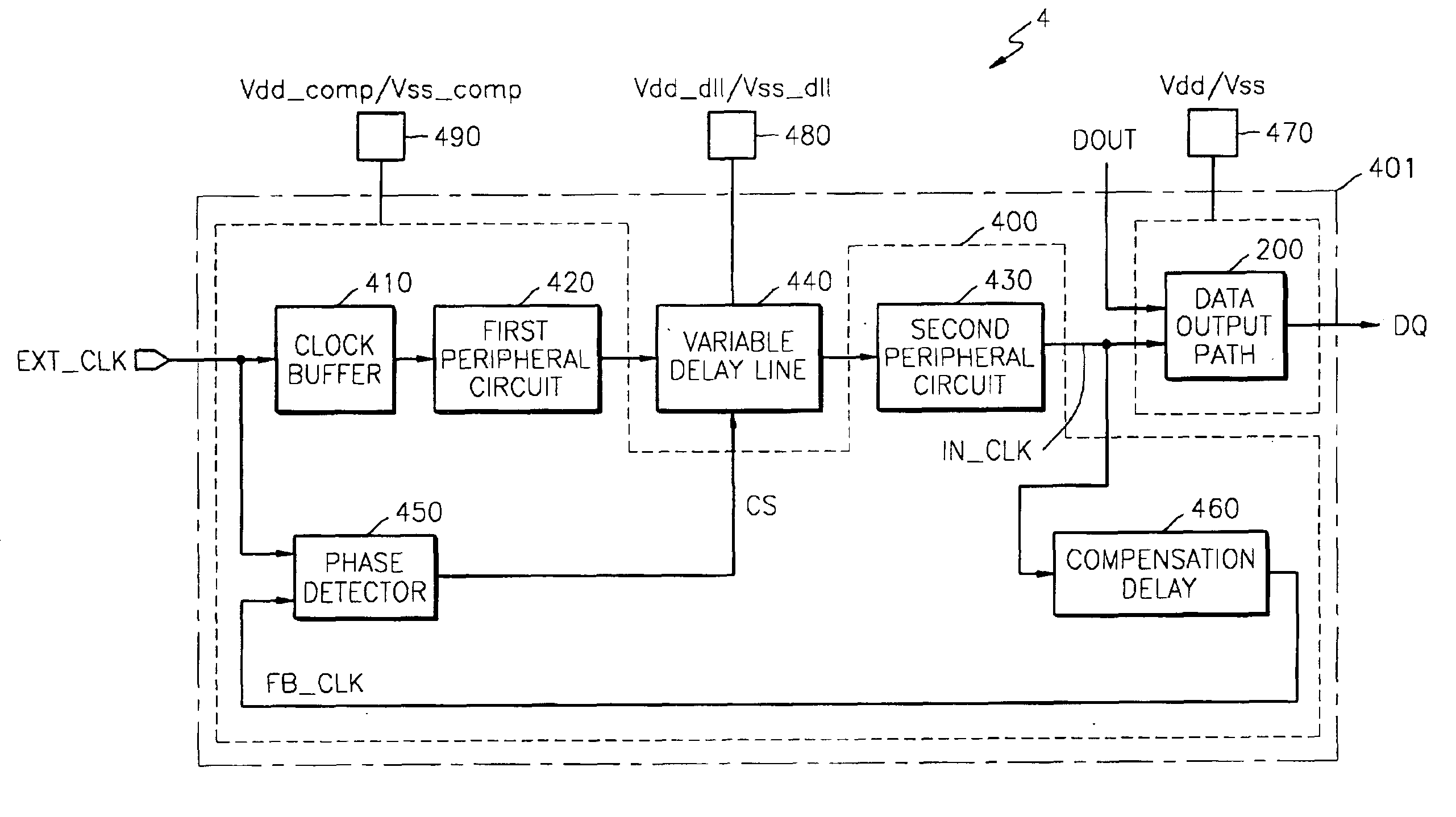
[0030]FIG. 4 is a block diagram illustrating portions of a semiconductor memory device 4 according to...


PUM


Abstract

A memory device includes first and second power supply pads configured to be connected to a power supply. The memory device further includes a data output circuit that receives power via the first power supply pad and outputs data responsive to an internal clock signal, and a delay-locked loop (DLL) circuit that receives power via the second power supply pad independently of the first power supply pad and that generates the internal clock signal responsive to an external clock signal.

Description

RELATED APPLICATION[0001]This application claims priority to Korean Patent Application 2002-8474, filed on Feb. 18, 2002, the contents of which are herein incorporated by reference in their entirety.BACKGROUND OF THE INVENTION[0002]The present invention relates to semiconductor (integrated circuit) memory devices, and more particularly, to semiconductor memory devices having a delay locked loop (DLL) for synchronizing output data to a clock.[0003]A typical DLL locks data output from a semiconductor memory device to an external clock signal. The DLL compares its output signal with the external clock signal, and increases or decreases its delay time to lock the output data to the external clock signal, so that the output timing of the data substantially matches that of the external clock. In order to precisely lock the output data of the memory device to the external clock, it is often necessary to estimate the delay in a data output path and compensate for the delay in a feedback loo...

Claims


Application Information

Patent Timeline
Patent Type & Authority Patents(United States)
IPC IPC(8): G11C7/00G11C7/22G11C8/00G11C11/401G11C11/407G11C11/4074G11C11/4076H03K5/13H03L7/00
CPCG11C7/22G11C7/222G11C2207/105G11C8/00
Inventor LIM, HYUN-WOOKCHUNG, DAE-HYUN
Owner SAMSUNG ELECTRONICS CO LTD
Why Eureka
Try Eureka