Multilayer field emission klystron

a field emission klystron and multi-layer technology, applied in the direction of klystrons, transit-tube vessels/containers, electric discharge tubes, etc., can solve the problems of difficult to tightly bunch beam electrons, large cavity gaps, and inability to meet the requirements of high-frequency applications, etc., to achieve the effect of relatively simple and straightforward fabrication and easy modification of power and frequency of operation

Inactive Publication Date: 2005-04-26
MOTOROLA SOLUTIONS INC
View PDF7 Cites 3 Cited by
  • Summary
  • Abstract
  • Description
  • Claims
  • Application Information

AI Technical Summary

Benefits of technology

[0007]In various representative aspects, the present invention provides a system and method for providing a multilayer field emission klystron suitably adapted for high frequency operation. An exemplary system and method for providing such a device is disclosed as comprising inter alia: a field emission cathode layer, a collector layer; an extraction layer; a control layer, an input cavity; an output cavity; several ceramic spacer layers dispose intermediately between the cathode and the collector; and optionally, several magnetic ceramic layers for beam forming and focusing. After the klystron's ceramic layers are assembled, the multilayer device may be fired to form a substantially monolithic structure capable of economical generation of millimeter wave RF energy in accordance with various aspects of the present invention. Fabrication is relatively simple and straightforward. Power and frequency of operation may be easily altered without fundamental design changes. Additional advantages of the present invention will be set forth in the Detailed Description which follows and may be obvious from the Detailed Description or may be learned by practice of exemplary embodiments of the invention. Still other advantages of the invention may be realized by means of any of the instrumentalities, methods or combinations particularly pointed out in the Claims.

Problems solved by technology

First, if the perveance is made high, there is an adverse impact on the efficiency of the device because the space-charge forces in the beam generally increase making it difficult to tightly bunch the electrons of the beam.
Therefore, the dimensions of these cavity gaps may be required to become extremely small in high frequency applications.
Notably, there are substantial deficiencies associated with the prior art's ability to provide methods for the manufacture of klystrons suitably adapted for high-frequency operation.
For example, U.S. Pat. No. 5,534,747 (Caruthers); U.S. Pat. No. 6,400,069 (Espinosa); U.S. Pat. No. 6,326,730 (Symons) and U.S. Pat. No. 5,796,211 (Graebner, et al.) generally describe conventional features of klystron design and construction, but do not address the problems of miniaturization and fabrication costs for the enablement of high frequency operation.
Consequently, conventional klystrons have not generally found use at frequencies above 26 GHz due to limitations inherent to existing vacuum device processing.

Method used


Image

  • Multilayer field emission klystron
  • Multilayer field emission klystron
  • Multilayer field emission klystron

Examples


Embodiment Construction

[0011]The following descriptions are of exemplary embodiments of the invention and the inventors' conceptions of the best mode and are not intended to limit the scope, applicability or configuration of the invention in any way. Rather, the following Description is intended to provide convenient illustrations for implementing various embodiments of the invention. As will become apparent, changes may be made in the function and / or arrangement of any of the elements described in the disclosed exemplary embodiments without departing from the spirit and scope of the invention.

[0012]A detailed description of an exemplary application, namely a system and method for field emission klystron operation at millimeter wave frequencies is provided as a specific enabling disclosure that may be readily generalized by skilled artisans to any application of the disclosed system and method for electron beam applications in accordance with various embodiments of the present invention.

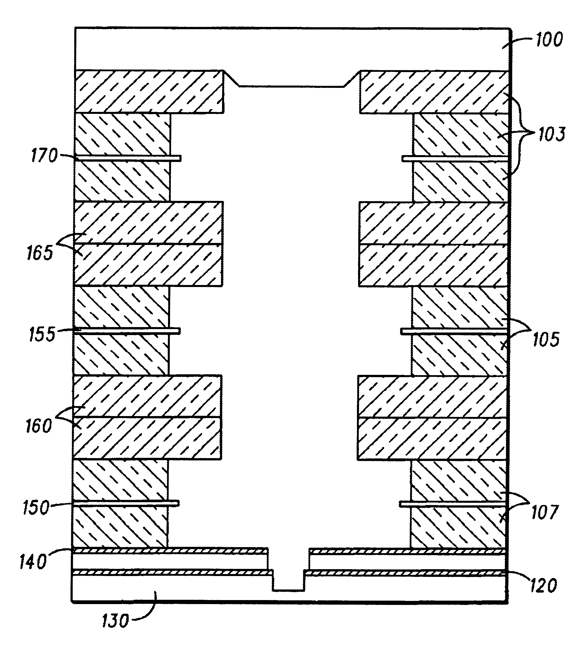
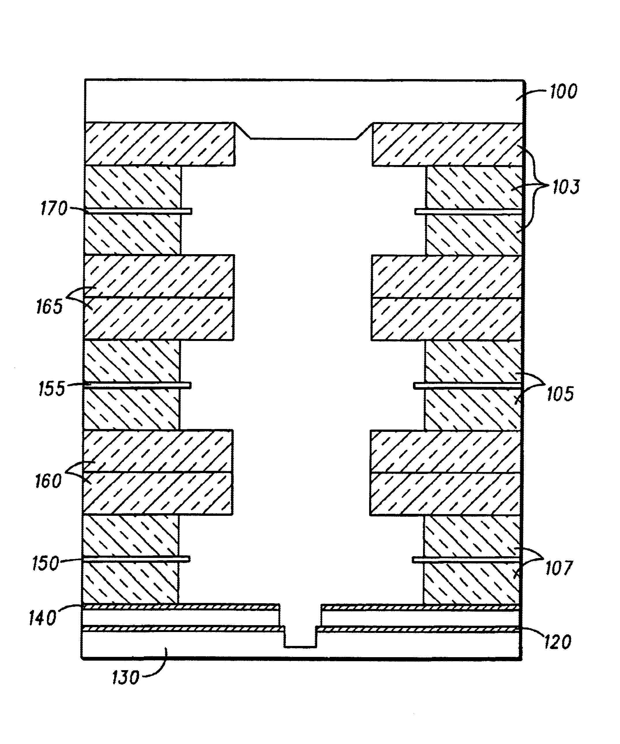
[0013]The FIGURE r...


PUM


Abstract

An exemplary system and method for providing a multi-layer klystron-type electron beam device for the generation and amplification of millimeter-wave electromagnetic radiation is disclosed as comprising inter alia: a cathode layer (130); a collector layer (100); an extraction layer (120); a control layer (140); an input cavity (150); an output cavity (170); several ceramic spacer layers (103, 105, 107) dispose intermediately between the cathode (130) and the collector (100); and optionally, several magnetic ceramic layers (160, 165) for beam forming and focusing. After the klystron's layers are assembled, the device may be fired to form a substantially monolithic structure.

Description

FIELD OF INVENTION[0001]The present invention generally concerns field emission electron beam devices; and more particularly, in various representative and exemplary embodiments, to low-power multilayer klystrons suitably adapted to provide high efficiency and wide bandwidth.BACKGROUND[0002]Linear beam electron devices are used in sophisticated communication and RADAR systems that generally require amplification of radio frequency (RF) or microwave electromagnetic radiation. A conventional klystron is an example of a linear beam electron device that has been used as a microwave amplifier. In a conventional klystron device, an electron beam originating from an electron gun may be caused to propagate through a drift tube that passes across a number of gaps, each gap corresponding to part of a resonant cavity of the klystron. The velocity of the electron beam is typically modulated by an RF input signal introduced at the first resonant cavity. The velocity modulation of the beam genera...

Claims


Application Information

Patent Timeline
Patent Type & Authority Patents(United States)
IPC IPC(8): H01J23/02H01J23/08H01J23/12H01J25/14
CPCH01J25/14H01J23/12
Inventor JOHNSON, SCOTT V.COLL, BERNARD F.DEAN, KENNETH A.
Owner MOTOROLA SOLUTIONS INC
Why Eureka
Try Eureka