Semiconductor device

Inactive Publication Date: 2005-05-03
LAPIS SEMICON CO LTD
View PDF10 Cites 16 Cited by
  • Summary
  • Abstract
  • Description
  • Claims
  • Application Information

AI Technical Summary

Benefits of technology

[0041]Accordingly, the cumulative number of chips per wafer can be improved, whereby an increase in fabrication costs can be suppressed.

Problems solved by technology

However, because the WCSPs that comprise the re-distribution wiring layer described above are packages whose outer dimensions are substantially the same as the outer dimensions of the semiconductor chip as described earlier, there are limits on the number of external terminals that can be arranged on the mount surface.
However, although setting the interval between external terminals at about 0.4 mm is technically feasible, such a practice is undesirable due to the requirement for a high density mounting technology during the mounting on the mount substrate.
Furthermore, in the case of a multiple pin class of about 300 pins, however narrow the external terminal interval may be, it is sometimes difficult to arrange the pins on the mount substrate.
However, since the inductance of the WB parts is high in the case of such structures in which the wire bonding method is normally adopted, impedance matching with the circuit in the semiconductor chip is problematic.
Furthermore, because a wiring substrate such as one comprising bonding pads is required, not only does this lead to a thick package, fabrication costs are also increased.
However, because the interval between pads (electrode pads) on the semiconductor chip is then equal to or less than 0.1 mm, an expensive build-up substrate is required, and the flip bonding processing takes a long time.
Hence such a method is not suited to mass production.
Further, also with the above-described MCPs, in the case of a structure that adopts the WB method, problems include increased inductance and an increase in the package external form and package thickness, and so forth, which are caused by the WB, as described earlier.
Moreover, even with the above-described package stacked-type MCPs, in the case of a structure that adopts the WB method, not only are there problems that include increased inductance and an increase in the package external form and package thickness, and so forth, which are caused by the WB, as described earlier, an increase in the number of pins of the MCP is also unsuitable because the MCP cannot be afforded a fan-in structure.

Method used


Image

  • Semiconductor device
  • Semiconductor device
  • Semiconductor device

Examples


first embodiment

[0057

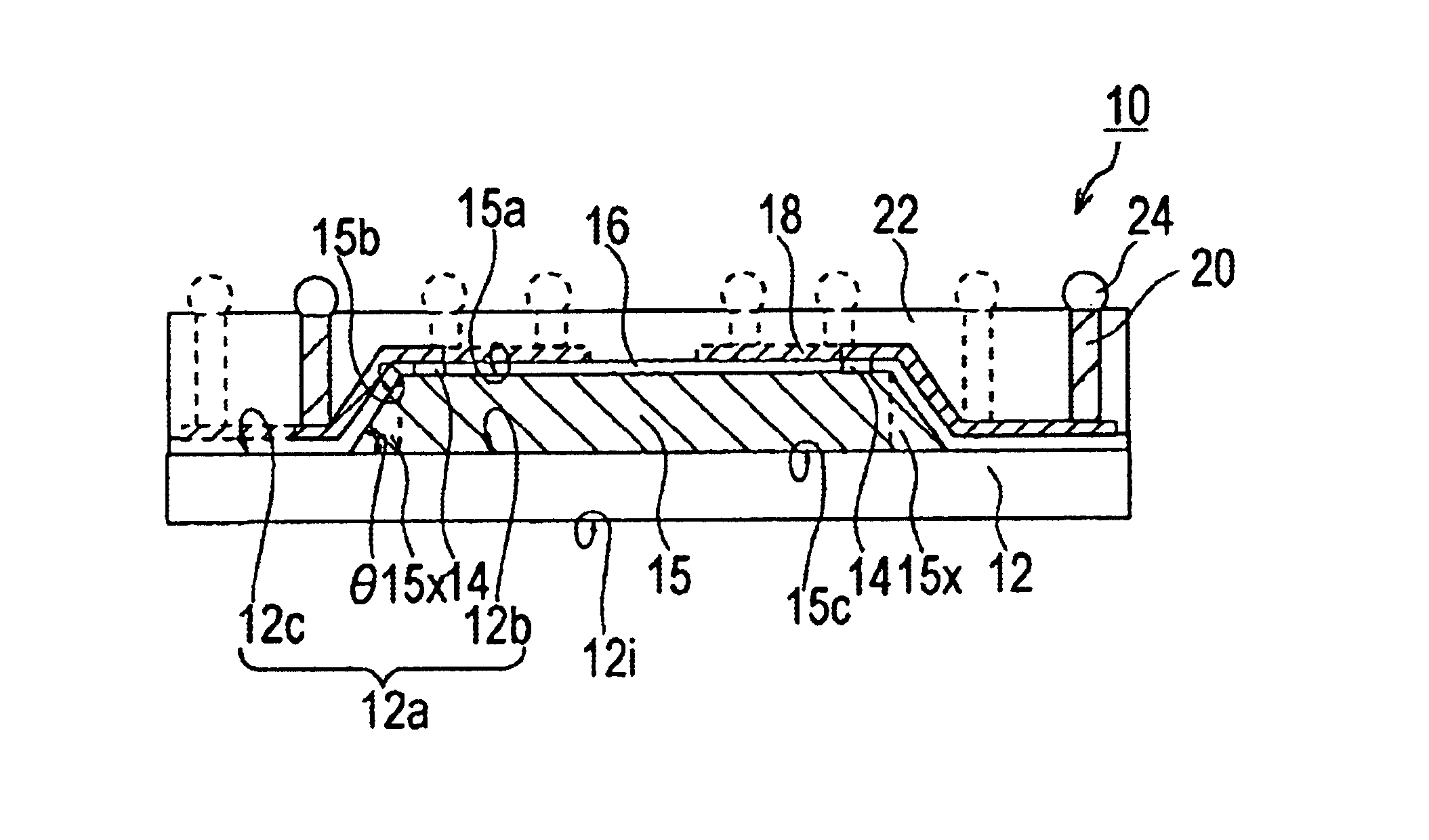
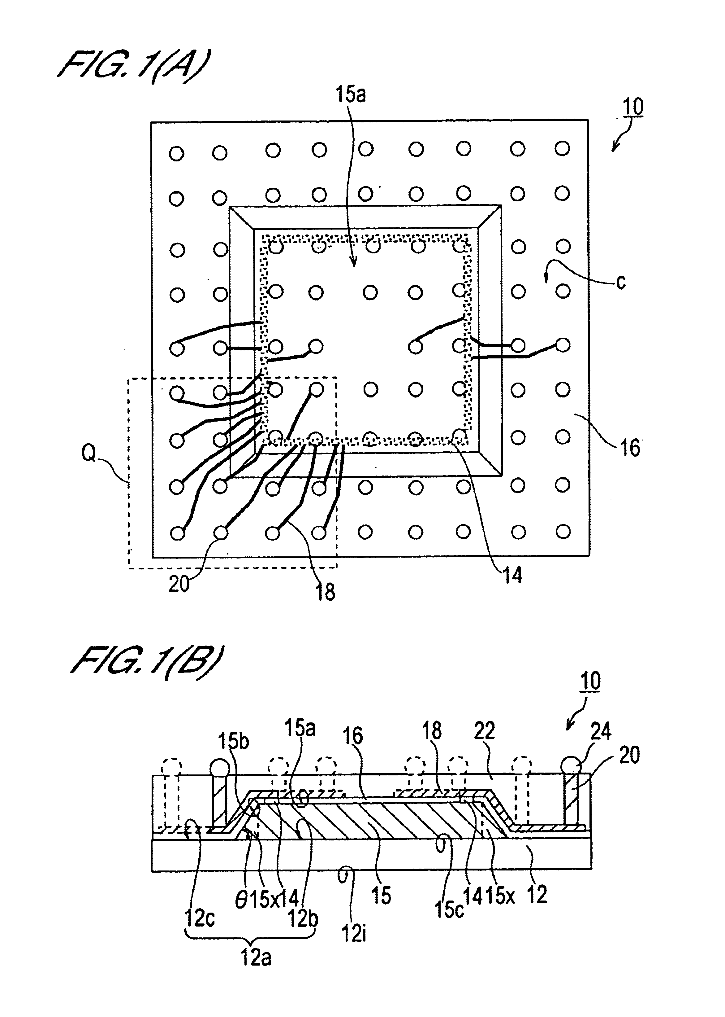
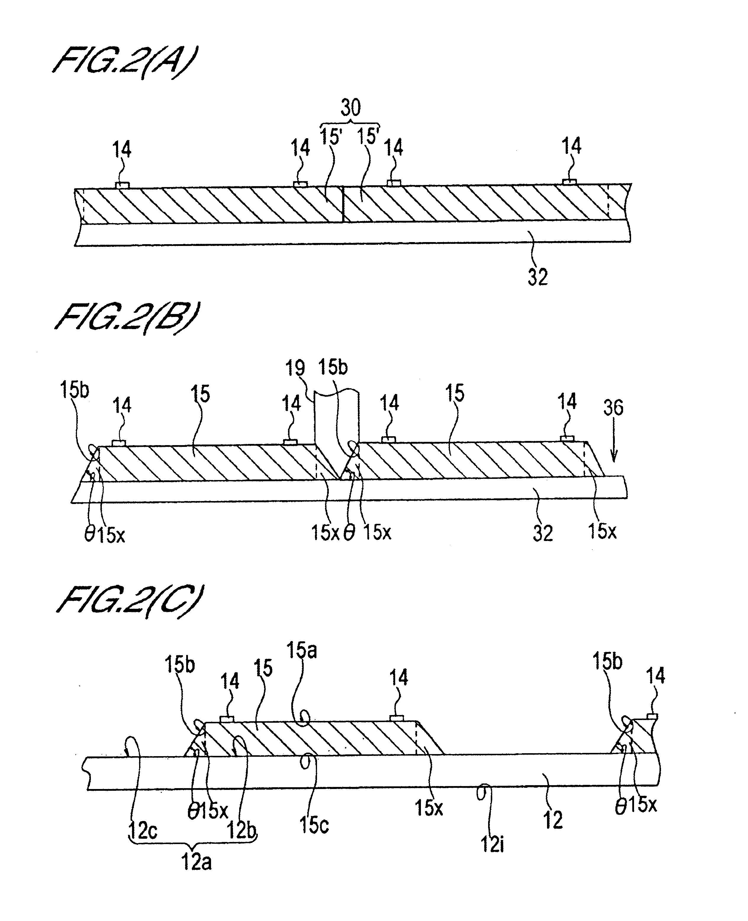
[0058]A description will now be provided for the semiconductor device and fabrication method thereof according to the first embodiment of the invention, with reference to FIGS. 1 to 3. FIG. 1(A) is an outline planar view of a semiconductor device 10 of this embodiment. Further, although FIG. 1(B) does not correspond with FIG. 1(A), FIG. 1(B) is a cross-sectional view in which, in order to describe the appearance of the connection between and disposition of the constituent elements of the semiconductor device 10, the connection between and disposition of these elements are modified and shown in outline. Further, in FIG. 1(A), there is no illustration of the external terminals and so forth formed on the post portions 20, and, with the exception of a region Q in this figure, the overview of part of first pads 14, a first wiring layer 18 and the post portions 20 does not include such an illustration (as is also the case for the embodiments below)

[0059]As shown in FIG. 1(A), the fir...

second embodiment

[0095

[0096]A description will now be provided for a semiconductor device 11 according to the second embodiment of the present invention, with reference to FIGS. 4(A) and 4(B).

[0097]The principal points of difference between the first and second embodiments are as follows. First, a through-hole 38 is formed as a perforation in the substrate 12 which is a semiconductor chip carrying portion, this through-hole 38 comprising a conductive portion 39 affording conduction between the two sides of the substrate 12, that is, from the third main surface 12a through to the fourth main surface 12i. The conductive portion 39 is electrically connected to the first wiring layer 18, and the substrate 12 comprises a wiring portion 27 that transects the regional part facing the first semiconductor chip 15, the wiring portion 27 being electrically connected to the first wiring layer 18. Further, constituent elements which are the same as those already described in the first embodiment are shown with t...

third embodiment

[0112

[0113]A description will now be provided for a semiconductor device 50 according to the third embodiment of the present invention, with reference to FIGS. 5 and 6.

[0114]In this embodiment, the main point of difference from the first embodiment is that the semiconductor chip carrying portion is a second semiconductor chip 44 which comprises circuit elements and that the second semiconductor chip 44 is electrically connected to the first wiring layer 18.

[0115]As shown in FIG. 5(A), the planar form of the second semiconductor chip 44 which is the semiconductor chip carrying portion is square. Fourth pads 45 comprising aluminum (Al) are arranged at predetermined intervals along the perimeter of the second semiconductor chip 44, on a mount surface 44a which constitutes the third main surface of the second semiconductor chip 44, and the fourth pads 45 are constituted so as to be electrically connected to the first wiring layer 18. Further, the placement quantity of the fourth pads 45...


PUM


Abstract

An object of the present invention is to provide a semiconductor device capable of adapting to an increase in the external terminals which can be arranged on the mount surface (a greater number of pins). A mesa-type semiconductor chip is mounted on a mount surface of a substrate which is a semiconductor chip carrying portion such that the side wall surface of the four side walls of the first semiconductor chip intersects the mount surface at an acute angle θ (0°<θ<90°). Further, a first pad formed on a main surface of the first semiconductor chip is electrically connected to a solder ball provided on an unmounted surface, via a first wiring layer, one end of which is connected to the first pad, and which extends along the main surface, the side wall surface, and the unmounted surface of the semiconductor chip.

Description

BACKGROUND OF THE INVENTION[0001]1. Field of the Invention[0002]The present invention relates to a semiconductor device with a package structure.[0003]2. Description of Related Art[0004]Recent years have witnessed an ever-increasing demand for miniaturization and an increase in the density of semiconductor devices that are mounted in electronic devices such as portable devices, as well as for higher frequency transmission signals. Accordingly, CSPs (Chip Size Packages) which are semiconductor devices packaged such that the external size thereof is substantially the same as the external size of the semiconductor chip have been attracting attention.[0005]With a view to reducing fabrication costs and so forth, recent years have more particularly seen the active development of WCSP (Wafer-level Chip Size Package) technology (for example, Nikkei Microdevices, February 1999 Edition, pages 48 to 56, FIGS. 1 and 4), which are CSPs produced by means of completion as far as the external termi...

Claims


Application Information

Patent Timeline
IPC IPC(8): H01L21/02H01L21/60H01L29/06H01L23/28H01L23/31H01L29/02H01L23/52H01L23/12
CPCH01L23/3128H01L29/0657H01L2224/24226H01L2224/24998H01L2924/01015H01L2924/01075H01L2224/82007H01L2924/01079H01L2924/10157H01L2924/15311H01L2924/19041H01L2924/30107H01L2924/3011H01L2924/01078
Inventor SHIZUNO, YOSHINORI
Owner LAPIS SEMICON CO LTD
Why Eureka
Try Eureka