Vertical Power MOSFET and IGBT Fabrication Process with Two Fewer Photomasks

Active Publication Date: 2011-12-22
LITTELFUSE INC
View PDF1 Cites 1 Cited by
  • Summary
  • Abstract
  • Description
  • Claims
  • Application Information

AI Technical Summary

Benefits of technology

[0006]This invention provides a method for manufacturing such devices using two fewer photo masks in the fabrication process of vertical power MOSFETs and insulated gate bipolar transistors (IGBTs). In general, requiring a larger number of photo masks causes increased fabrication costs. This invention eliminates at least two masking steps from the typical fabrication process. p

Problems solved by technology

In general, requiring a larger number of photo masks causes increased fabrication costs.
The complexity of the proc

Method used


Image

  • Vertical Power MOSFET and IGBT Fabrication Process with Two Fewer Photomasks
  • Vertical Power MOSFET and IGBT Fabrication Process with Two Fewer Photomasks
  • Vertical Power MOSFET and IGBT Fabrication Process with Two Fewer Photomasks

Examples


Embodiment Construction

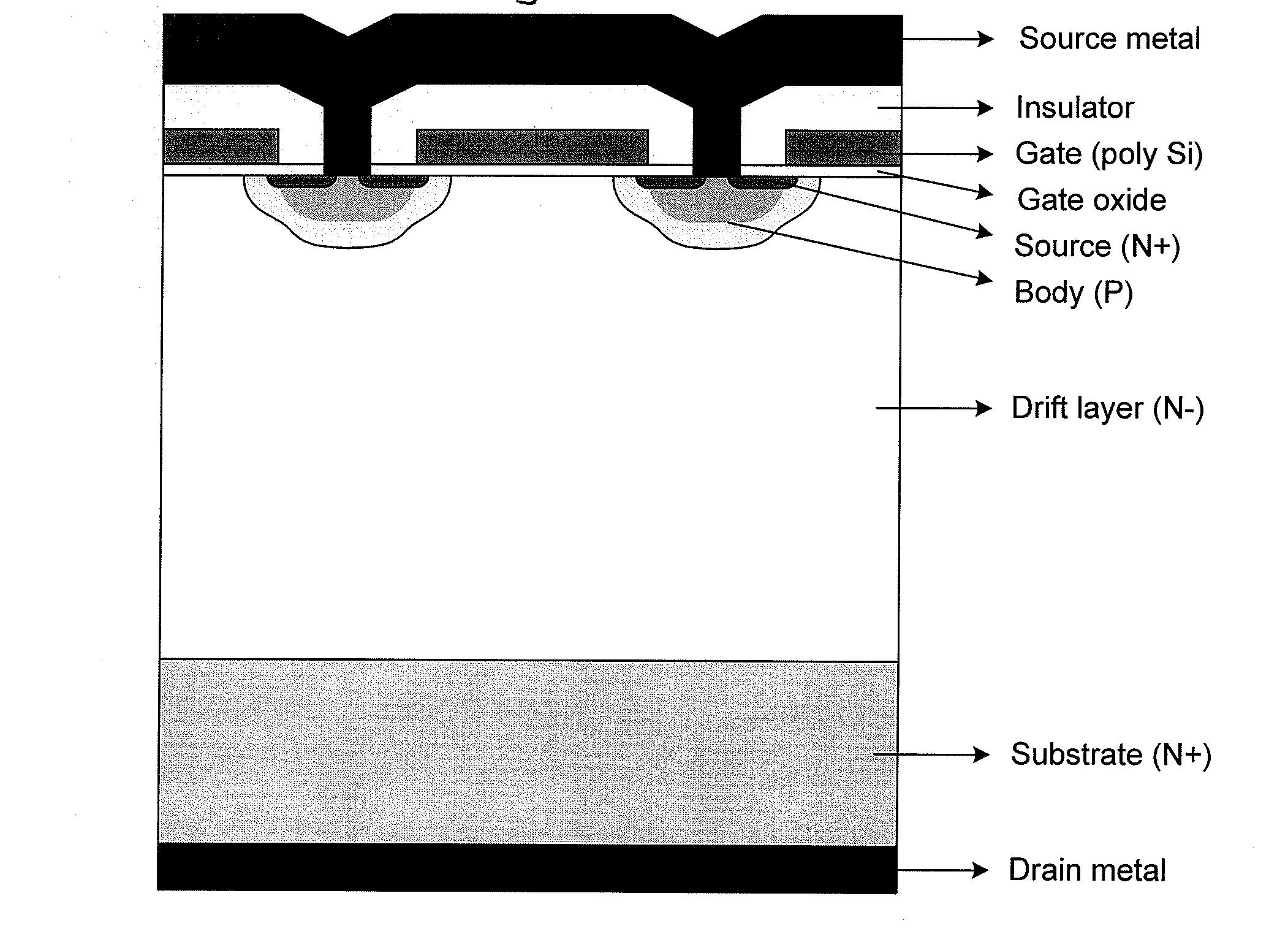
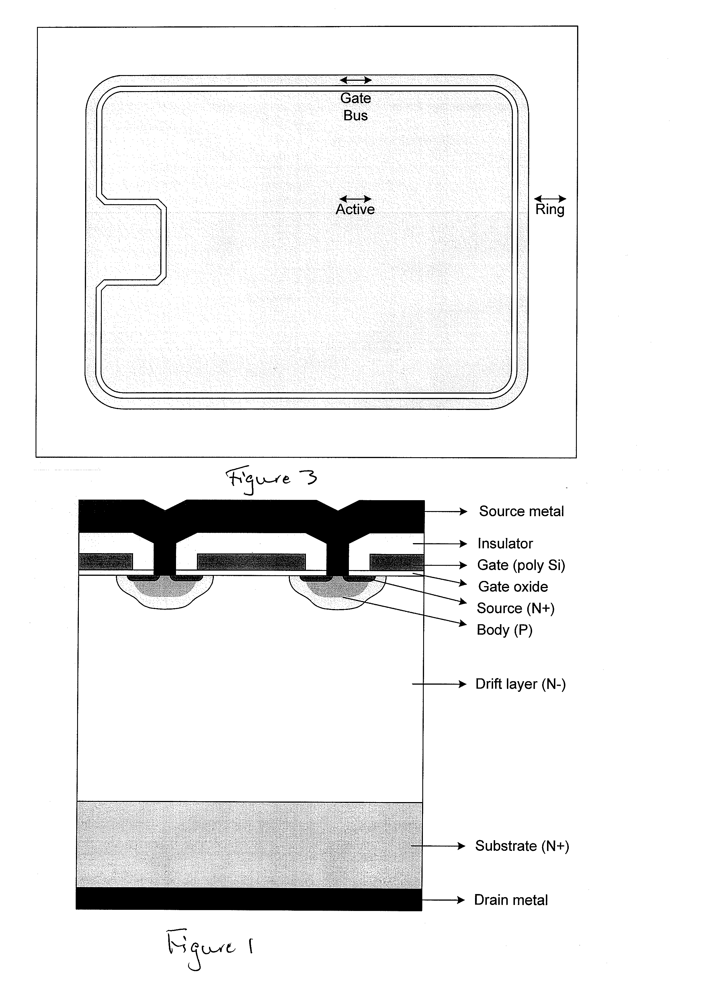
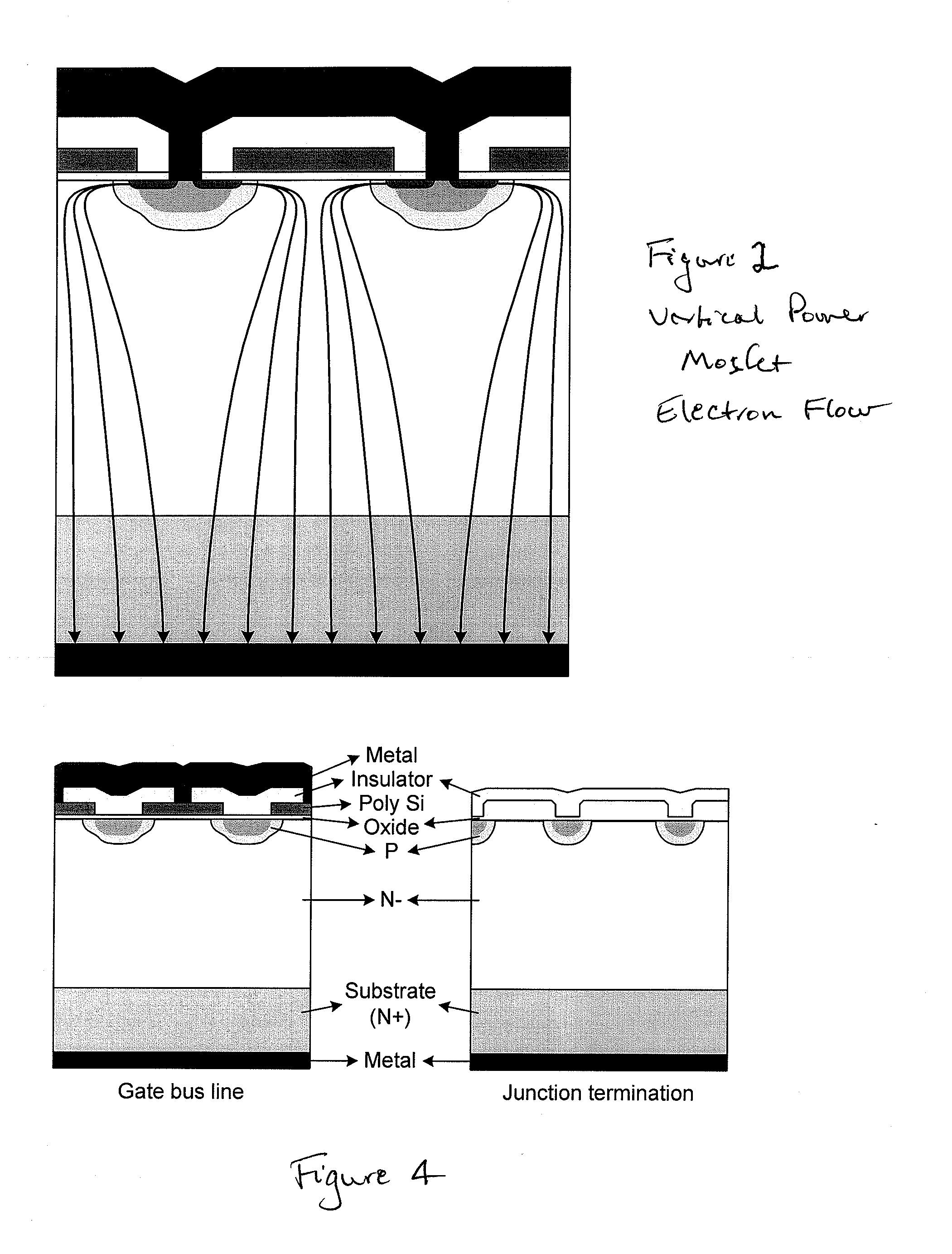
[0091]A typical fabrication process for vertical power MOSFETs and IGBTs has 7 masks. The [Ring] mask defines the junction termination rings. The [Poly] mask defines the poly silicon gate and P well. The [P+] mask defines the highly doped region in the P well. The [N+] mask defines the source. The [Contact] mask defines the metal contacts for source and gate. The [Metal] mask shapes the source metal and gate bus line. The [Pad] mask is used for passivation, and is sometimes omitted.

[0092]This invention provides a fabrication process having 2 fewer photo masks than the typical conventional process. The first mask [Poly] defines the silicon gate, P well and junction termination ring. The second mask [Multipurpose] plays an important role of this invention. This mask eliminates unnecessary polysilicon in the junction termination area causing its removal. It also defines the N+ source, and the highly doped region in P well. From [Contact] mask, this process is similar to the conventiona...


PUM


Abstract

A process for fabrication of a power semiconductor device is disclosed in which a single photomask is used to define each of p-conductivity well regions and n-conductivity type source regions. In the process a single photomask is deposited on a layer of polysilicon on a wafer, the polysilicon layer is removed from first regions of the power semiconductor device where the p-conductivity well regions and the n-conductivity type source regions are to be formed, and both p-conductivity type and n-conductivity type dopants are introduced into the wafer through the first regions.

Description

CROSS-REFERENCE TO RELATED APPLICATION[0001]This application claims priority to U.S. Provisional Patent Application No. 61 / 347,793, filed May 24, 2010, which is incorporated by reference herein for all purposes.BACKGROUND OF THE INVENTION[0002]Its high switching speed, simple gate drive and wide safe operating area, have made vertical power MOSFETs a common switching device for modern power electronics. Because of its high current density, moderate switching speed, simple gate drive, and wide safe operating area, the IGBT is now also in widespread use for high power applications.[0003]FIG. 1 illustrates a typical structure of vertical power MOSFET. The drain is at the bottom and the source is at the top. The current flows from bottom to top. Almost all of the area is used for current flow. The heat is dissipated through the entire bottom area, typically attached to a thick lead frame. In the blocking state, the voltage between the gate and the source is less than the threshold volta...

Claims


Application Information

Patent Timeline
IPC IPC(8): H01L21/336
CPCH01L29/0619H01L29/1095H01L29/41766H01L29/66666H01L29/66727H01L29/7395H01L29/7811H01L29/66333
Inventor SEOK, KYOUNG WOOKCHOI, JAE YONGTSUKANOV, VLADIMIR
Owner LITTELFUSE INC
Why Eureka
Try Eureka