Process for disengaging semiconductor die from an adhesive film

a technology of adhesive film and semiconductor die, which is applied in the direction of soldering apparatus, mechanical control devices, instruments, etc., can solve the problems of reducing yield, increasing processing costs, and prone to problems on the substrate of the di

Inactive Publication Date: 2005-05-10
NXP USA INC
View PDF19 Cites 129 Cited by
  • Summary
  • Abstract
  • Description
  • Claims
  • Application Information

AI Technical Summary

Problems solved by technology

Functional die damaged during these operations unnecessarily increase processing costs and reduce yield.
One particular type of die substrate susceptible to problems during pre-packaging operations includes gallium arsenide (GaAs).
Crystalline GaAs is brittle and predisposed to chipping and cracking.
However, increased performance demands are imposing increased heat dissipation requirements, which in turn are forcing gallium arsenide chip manufacturers to consider designs wherein GaAs substrate thicknesses are on the order of 2-mil or less.
If detected, the fractures result in die scrap.
If undetected, the fractures pose a problem with device reliability.

Method used


Image

  • Process for disengaging semiconductor die from an adhesive film
  • Process for disengaging semiconductor die from an adhesive film
  • Process for disengaging semiconductor die from an adhesive film

Examples


Embodiment Construction

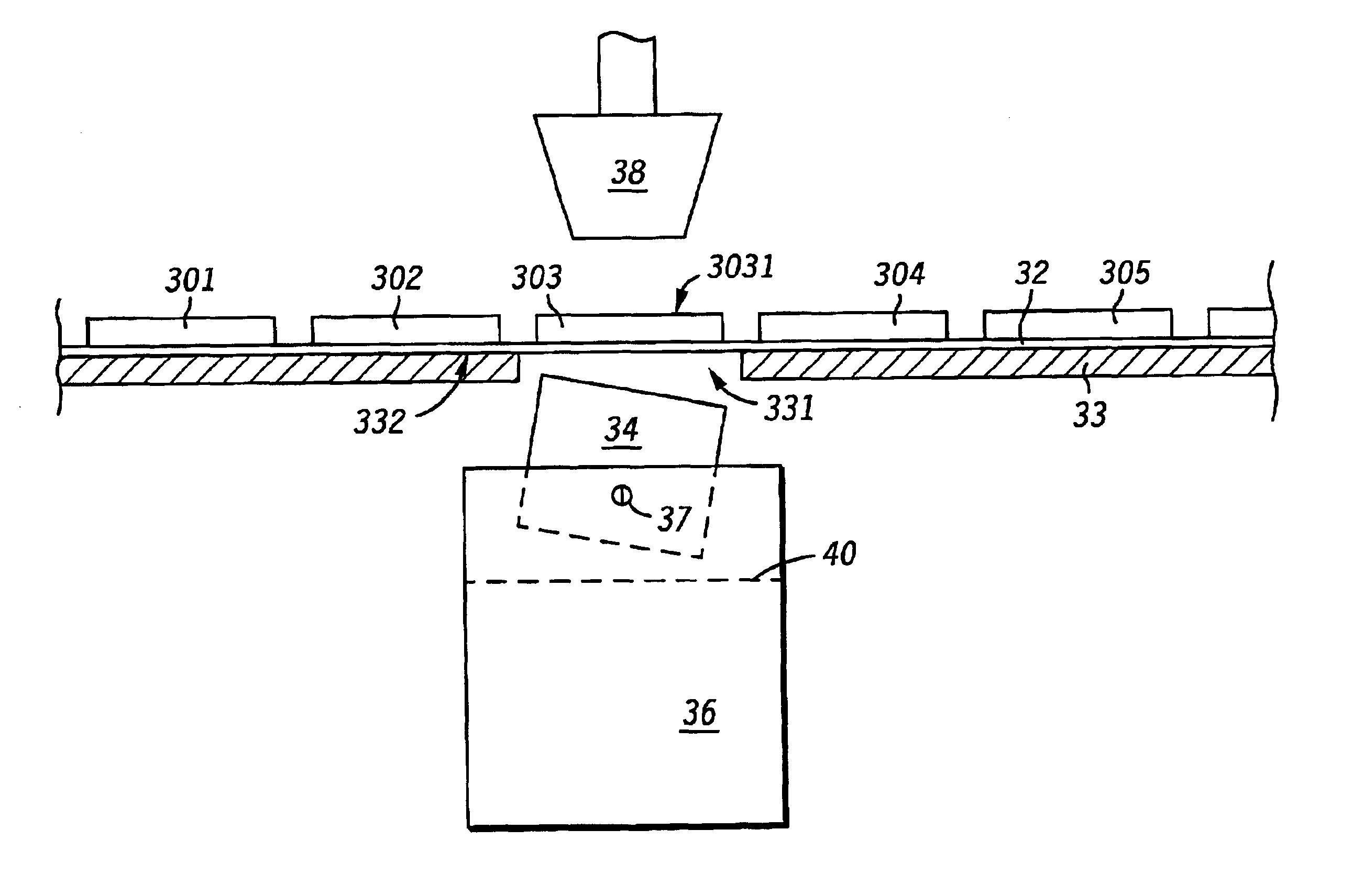
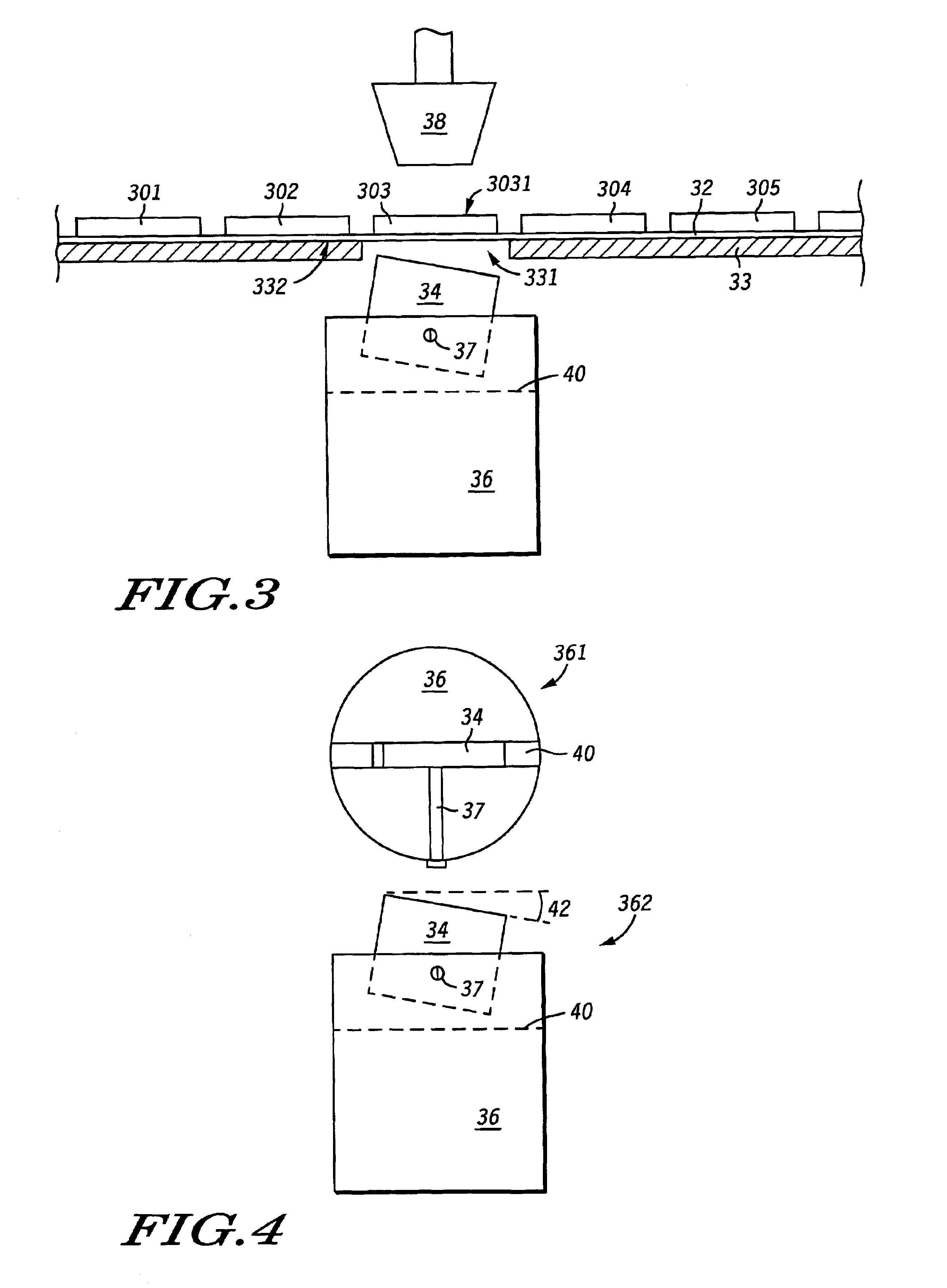
[0010]The present invention contemplates a method and apparatus for removing die from an adhesive film during a die attach operation. The apparatus includes a blade mechanically coupled to a blade holder, wherein the blade is inclined relative to the primary surface of the semiconductor die. The method further comprises using the blade to lift the semiconductor die while it is attached to the adhesive tape to assist in its disengagement. The blade facilitates peeling of the semiconductor die from the adhesive tape while distributing mechanical stresses exerted on the semiconductor die during the lifting operation across the surface area of the semiconductor die thereby resulting in reduced die fractures. Embodiments of the present invention will now be disclosed in greater detail with reference to the accompanying FIGS. 3-10.

[0011]FIG. 3 illustrates a cross-sectional view of a die picking system illustrating an embodiment of the present invention. Included in FIG. 3 are a plurality ...


PUM

PropertyMeasurementUnit
thicknessaaaaaaaaaa
thicknessaaaaaaaaaa
radiusaaaaaaaaaa

Abstract

An apparatus and method for separating a semiconductor die (303) from an adhesive tape (32) are disclosed. The apparatus includes a blade (34) mechanically coupled to a blade holder (36), wherein the blade (34) is inclined relative to the primary surface of the semiconductor die (303). The method further comprises lifting the semiconductor die (303) while it is attached to the adhesive tape (32) to assist disengagement. The blade (34) facilitates peeling of the semiconductor die (303) from the adhesive tape (32) while distributing stress exerted on the semiconductor die (303) over a larger surface area resulting in reduced die fractures (20).

Description

FIELD OF THE INVENTION[0001]The present invention relates generally to semiconductor manufacturing and more particularly to a process and apparatus for picking die during a die attach operation.BACKGROUND OF THE INVENTION[0002]Pre-packaging operations of IC chips, which include operations such semiconductor substrate (wafer) mounting, wafer sawing, die separation, die transfer, and die attach are critical operations which demand care while handling wafers and their respective dice and die. Functional die damaged during these operations unnecessarily increase processing costs and reduce yield. One particular type of die substrate susceptible to problems during pre-packaging operations includes gallium arsenide (GaAs). Crystalline GaAs is brittle and predisposed to chipping and cracking.[0003]In a typical pre-packaging operation, after wafers are sorted, they are mounted on adhesive tape. The adhesive tape provides support for the wafers during wafer saw, die transfer, and the die att...

Claims


Application Information

Patent Timeline
Patent Type & Authority Patents(United States)
IPC IPC(8): H01L21/00
CPCH01L21/67092H01L21/67132H01L2221/68322Y10S156/943Y10S156/932Y10T29/4913Y10T156/1983Y10T29/49815Y10T29/49798Y10T29/53274Y10T29/49117
Inventor YEE, LUP KWEUNBELMAS, DARRELL JACOB
Owner NXP USA INC
Why Eureka
Try Eureka