

Semiconductor device fabricating method and treating liquid
a technology of semiconductor devices and fabrication methods, applied in semiconductor devices, semiconductor/solid-state device details, electrical devices, etc., can solve problems such as easy oxidation of cu wiring in the via
- Summary
- Abstract
- Description
- Claims
- Application Information
AI Technical Summary
Benefits of technology
Problems solved by technology
Method used
Image

Examples
first embodiment
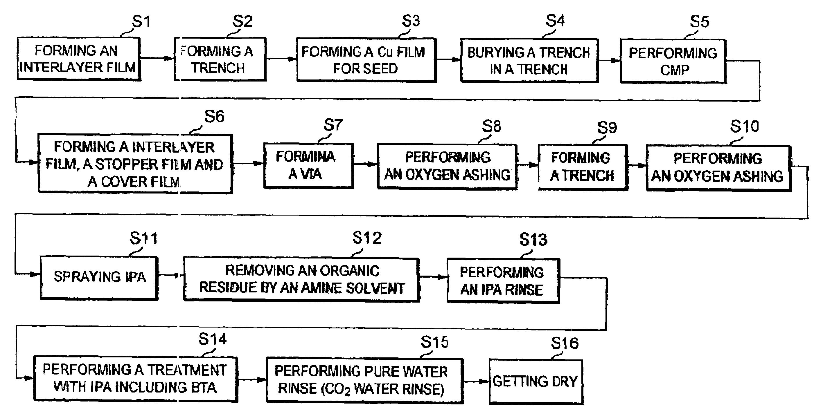
[0072]As described above, in the first embodiment, the semiconductor device is cleaned with the IPA as a nonaqueous solvent in step S11. Electric charges accumulated onto the interlayer film can be discharged without eluting the Cu constructing the Cu wiring 4. When rinsing the semiconductor device with pure water or CO 2 water in step S15, the Cu constructing the Cu wiring 4 can thus be prevented from being eluted. The treating liquid is sprayed to the semiconductor device in step S14 to form the BTA film 16 on the exposed part 4a of the Cu wiring 4 in the via 11. In the semiconductor device rinsing process with pure water or CO2 water in step S15, the Cu constructing the Cu wiring 4 can thus be prevented from being eluted. The exposed part 4a of the Cu wiring 4 after drying can be also prevented from being oxidized. This can increase time during which the cleaned semiconductor device can be maintained in a normal state, that is, allowable time. Time from the cleaning process to th...
second embodiment
[0086]As described above, according to the present invention, since the semiconductor device is cleaned by IPA as a nonaqueous solvent at steps S29 and S36. Electric charges accumulated onto the inter layer film can be released with out eluting metal constituting the Cu wiring 32 and 39.
[0087]Further, according to the second embodiment of the present invention, since the semiconductor device is formed by a process for cleaning with IPA as a final cleaning process without a process for cleaning with pure water or CO2 water. Therefore, the metal. constructing the Cu wiring 32 and 39 can be prevented from being eluted due to the process for cleaning with pure water or CO 2 water. As a result, as described in the first embodiment, it is not necessary to form a BTA film on an exposed part of the Cu wiring in the via. The semiconductor device fabricating process is simplified.
[0088]Next, the third embodiment of the present invention will be described. FIG. 13 is a flowchart showing a semi...
PUM
 Abstract
Description
Claims
Application Information