Contact member stacking system and method

Inactive Publication Date: 2005-05-17
TAMIRAS PER PTE LTD LLC
View PDF2 Cites 2 Cited by
  • Summary
  • Abstract
  • Description
  • Claims
  • Application Information

AI Technical Summary

Benefits of technology

[0013]Methods for creating stacked integrated circuit modules are provided that provide reasonable cost, mass production techniques to produce modules. In a preferred method, a carrier frame of lead frame material is configured to present an opening into which opening project plural lead-like contact members that correspond to the leads of an IC element. The cont

Problems solved by technology

Many techniques add excessive height to the stack.
Most have deficiencies that a

Method used


Image

  • Contact member stacking system and method
  • Contact member stacking system and method
  • Contact member stacking system and method

Examples


Embodiment Construction

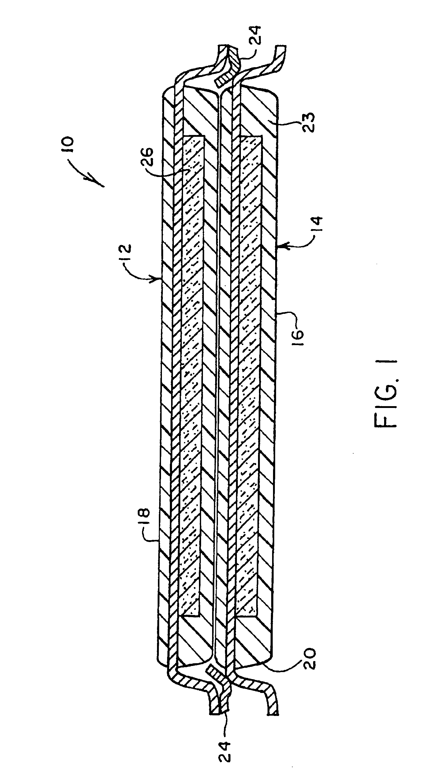
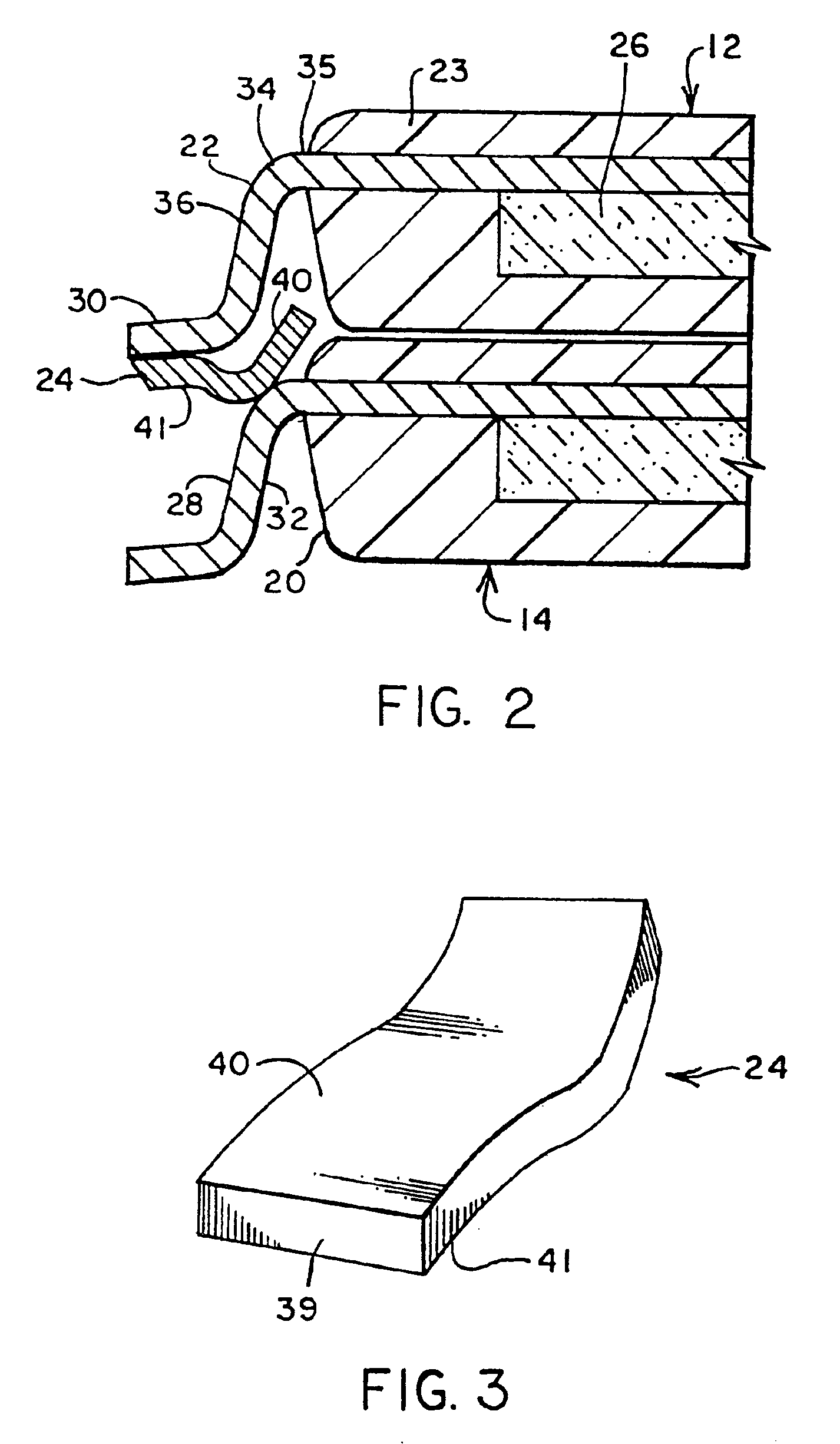
[0027]FIG. 1 depicts a high-density memory module 10 devised in accordance with the present invention. The present invention is adaptable to a variety of IC circuits and, in its preferred implementation, memory circuits of a variety of capacities. Module 10 is created with upper IC 12 and lower IC 14. Each of ICs 12 and 14 are, in the depicted preferred embodiment, plastic encapsulated memory circuits disposed in thin small outline packages known as TSOPs. Other package types may be used with the present invention as well as packaged circuits other than memories, but, as described here as preferred examples, the invention is advantageously implemented with memories in TSOP packaging. Each IC has a lower surface 16, upper surface 18 and periphery 20. Each of ICs 12 and 14 include an integrated circuit 26 encapsulated by a plastic body 23. As shown, contact members 24 provide connection between corresponding leads on ICs 12 and 14.

[0028]In this embodiment, due to the configuration of ...


PUM


Abstract

A system and method for selectively stacking and interconnecting individual integrated circuit devices to create a high-density integrated circuit module. In a preferred embodiment, conventional thin small outline packaged (TSOP) memory circuits are vertically stacked one above the other. The constituent IC elements act in concert to provide an assembly of memory capacity approximately equal to the sum of the capacities of the ICs that constitute the assembly. The IC elements of the stack are electrically connected through individual contact members that connect corresponding leads of IC elements positioned adjacently in the stack. In a preferred embodiment, the contact members are composed of lead frame material. Methods for creating stacked integrated circuit modules are provided that provide reasonable cost, mass production techniques to produce modules. In a preferred method, a carrier frame of lead frame material is configured to present an opening into which opening project plural lead-like contact members that correspond to the leads of an IC element. The contact members contact the leads of the lower IC element of the stack while the leads of the upper IC of the assembly contact the upper surfaces of the contact members. The stack is assembled using typical surface mount equipment and, after assembly, the carrier portion of the frame is removed to leave the plurality of contact members in place between selected leads.

Description

CROSS REFERENCE TO RELATED APPLICATIONS[0001]This application is a continuation application of U.S. application Ser. No. 10 / 092,104 filed on Mar. 06, 2002 now U.S. Pat. No. 6,806,120, pending, which is a divisional of U.S. patent application Ser. No. 09 / 819,171, filed Mar. 27, 2001, issued as U.S. Pat. No. 6,462,408. U.S. patent application Ser. No. 10 / 092,104 and U.S. patent application Ser. No. 09 / 819,171 are incorporated by reference for all purposes.TECHNICAL FIELD OF THE INVENTION[0002]The present invention relates to aggregating integrated circuits and, in particular, to stacking integrated circuits.BACKGROUND OF THE INVENTION[0003]A variety of techniques are used to stack integrated circuits. Some require that the circuits be encapsulated in special packages, while others use circuits in conventional packages. In some cases, the leads alone of packaged circuits have been used to create the stack and interconnect its constituent elements. In other techniques, structural elemen...

Claims


Application Information

Patent Timeline
IPC IPC(8): H01L25/10
CPCH01L25/105H01L2225/1029H01L2225/107H01L2225/1005H01L2924/0002H01L2924/00
Inventor WEHRLY, JR., JAMES DOUGLAS
Owner TAMIRAS PER PTE LTD LLC
Why Eureka
Try Eureka