Circuit analysis and manufacture using electric field-induced effects

Inactive Publication Date: 2005-05-17
GLOBALFOUNDRIES INC
View PDF11 Cites 8 Cited by
  • Summary
  • Abstract
  • Description
  • Claims
  • Application Information

AI Technical Summary

Benefits of technology

[0013]The above summary of the present invention is not intended to describe each illustrated embodiment or every implementat

Problems solved by technology

In addition, such devices often require manufacturing processes that are highly complex and expensive.
Directly accessing circuitry for device testing and analysis is difficult for several reasons.
For instance, in high-density circuit applications, it is difficult to accurately navigate stimulus sources to particular circuit nodes.
In addition, it is sometimes necessary to destroy a portion of the die in order to access circuit nodes, such as when accessing circuitry in a conventional die via a die passivation layer.
Transistors and other circuitry near the circuit side are not readily accessible for testing, modification, or other purposes due to this face-down orientation.
However, direct access to circuitry for analysis of SOI structure involves milling through the insulator, which can damage circuitry or other structure in the device.
Such damage can alter the characteristics of the device and render analysis of the device inaccurate.
In addition, the milling process can be time-consuming, difficult to control and expensive.
The difficulty, cost, and destructive aspects of existing methods for testing integrated circuits are impediments to the growth and improvement of semiconductor technologies, including those involving flip-chip structures, conventional structures and SOI structures.

Method used


Image

  • Circuit analysis and manufacture using electric field-induced effects
  • Circuit analysis and manufacture using electric field-induced effects
  • Circuit analysis and manufacture using electric field-induced effects

Examples


Embodiment Construction

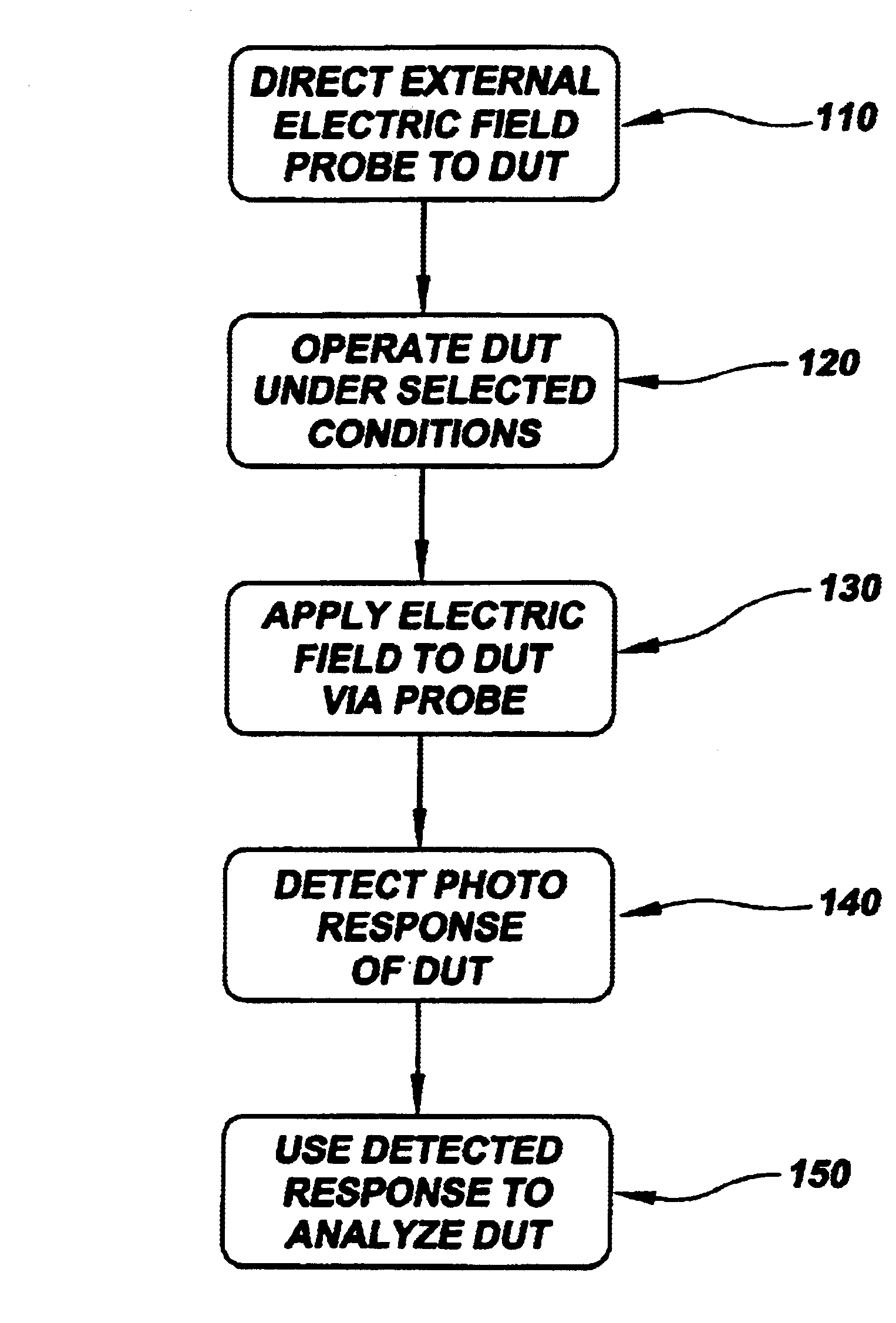
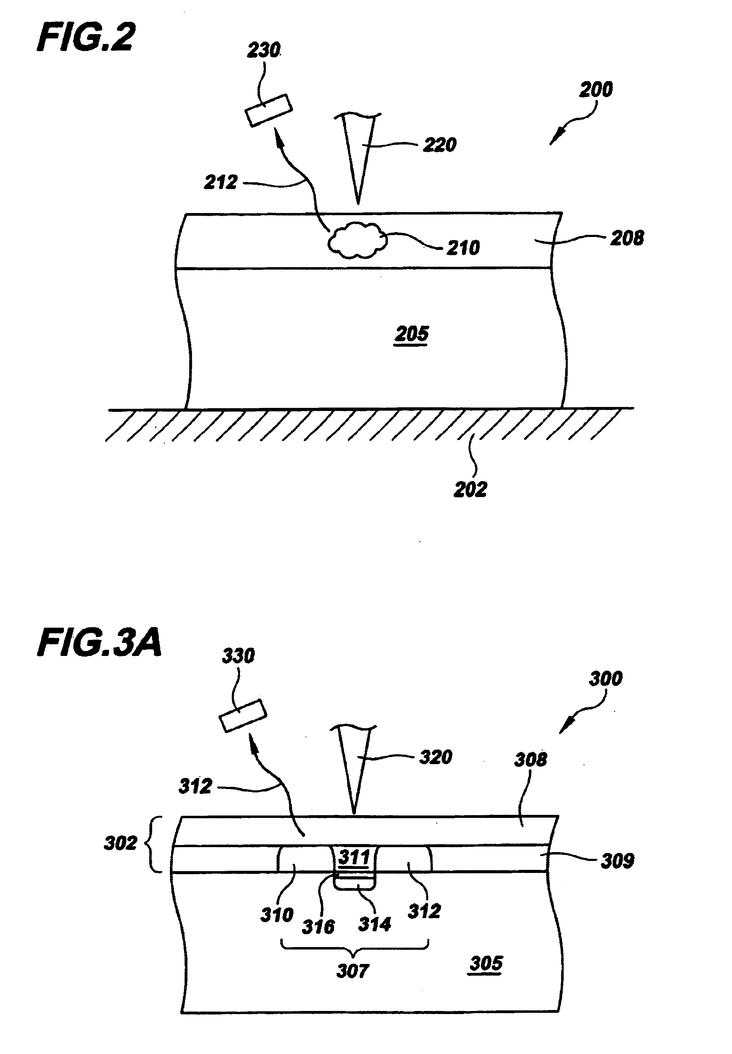
[0021]The present invention is believed to be applicable to a variety of different types of semiconductor devices, and has been found to be particularly suited for devices benefiting from analysis without necessarily directly contacting circuitry in the device. While the present invention is not necessarily limited to such devices, various aspects of the invention may be appreciated through a discussion of exemplary implementations using this context.

[0022]According to an example embodiment of the present invention, an electric field is applied to a semiconductor die using an external source, and a photoemission response of the die to the externally-applied electric field is detected. The electric field is applied to one or more circuit nodes in the die by directing the external source to the circuit node. The source is positioned to stimulate a circuit node in the die, and in one implementation, is scanned over several circuit nodes in the die. The stimulation causes a state change...


PUM


Abstract

Circuitry within a semiconductor die is analyzed by applying an electric field without necessarily directly accessing the circuitry. According to an example embodiment of the present invention, an electric field is applied to a semiconductor die and used to stimulate circuitry therein. A photoemission response of the die to the electric field is detected and used to detect an electrical characteristic of the die. This is particularly useful in applications where it is desired to direct stimulation to the die from an external source and to also externally detect a response of the die to the stimulation. In this manner, the die can be tested without necessarily directly contacting the die and, when the electric field is applied in a scanning mode over the die, can be effected without necessarily knowing the location of a defect in the die.

Description

FIELD OF THE INVENTION[0001]The present invention relates generally to semiconductor devices and their fabrication and, more particularly, to testing and defect analysis of semiconductor dies.BACKGROUND OF THE INVENTION[0002]Recent technological advances in the semiconductor industry have permitted highly functional, high-density circuit arrangements for integrated circuits, microprocessors and other semiconductor device applications. A by-product of such high functionality and high density is an increased demand for products employing these devices for use in numerous applications. As the use of these devices has become more prevalent, the demand for faster operation and better reliability of the devices has also increased. In addition, such devices often require manufacturing processes that are highly complex and expensive.[0003]As the manufacturing processes for semiconductor devices and integrated circuits increase in difficulty, methods for testing and debugging these devices b...

Claims


Application Information

Patent Timeline
IPC IPC(8): G01R31/311
CPCG01R31/311
Inventor BRUCE, MICHAEL R.GORUGANTHU, RAMA R.
Owner GLOBALFOUNDRIES INC
Why Eureka
Try Eureka