Method of selective removal of SiGe alloys

a technology of sige alloys and alloys, applied in the direction of semiconductor devices, basic electric elements, electrical equipment, etc., can solve the problems of low power, high speed, and low noise requirements, and achieve the effect of reducing the number of mosfet devices, and reducing the cost of mosfet devices

Inactive Publication Date: 2005-05-31
TAIWAN SEMICON MFG CO LTD
View PDF82 Cites 128 Cited by
  • Summary
  • Abstract
  • Description
  • Claims
  • Application Information

AI Technical Summary

Problems solved by technology

These low power, high speed, and low noise requirements present a significant design challenge both at the circuit design and at the transistor design level.
Analog MOSFET devices, which run on analog signals, typically exhibit noise problems because noise is induced at high frequency when carriers scatter along the Si / SiO2 interface of a traditional MOSFET device.
Unfortunately, it is difficult and expensive to integrate both bipolar and MOSFET devices on a single substrate.
While it is possible to build surface channel devices and buried channel devices on the same substrate, the manufacturing process requires complex and extensive process capabilities.
For example, use of ion implantation to populate the buried channel requires counterdoping of the layers above the buried channel, and also requires extensive masking steps, adding to the cost and complexity of the overall manufacturing process.
Furthermore, the excessive doping required to populate a buried conduction layer within a conventional silicon substrate places fundamental limitations on the performance of such a device.
Further, the use of strained semiconductor devices presents particular problems to the formation of surface channel devices and buried channel devices on the same substrate.
For example, the different layers of a strained semiconductor heterostructure may oxidize or become doped sufficiently differently that device formation procedures are compromised.
Moreover, with high thermal budget oxidation, the thin strained semiconductor channels may be destroyed by significant interdiffusion during the high temperature oxidation steps.

Method used


Image

  • Method of selective removal of SiGe alloys
  • Method of selective removal of SiGe alloys
  • Method of selective removal of SiGe alloys

Examples


Embodiment Construction

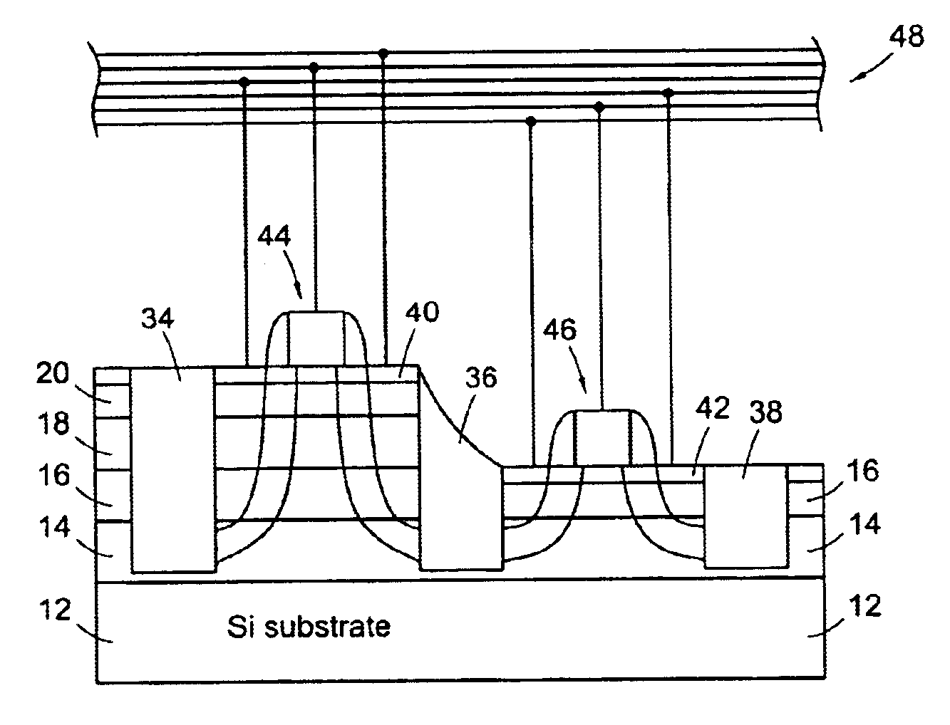
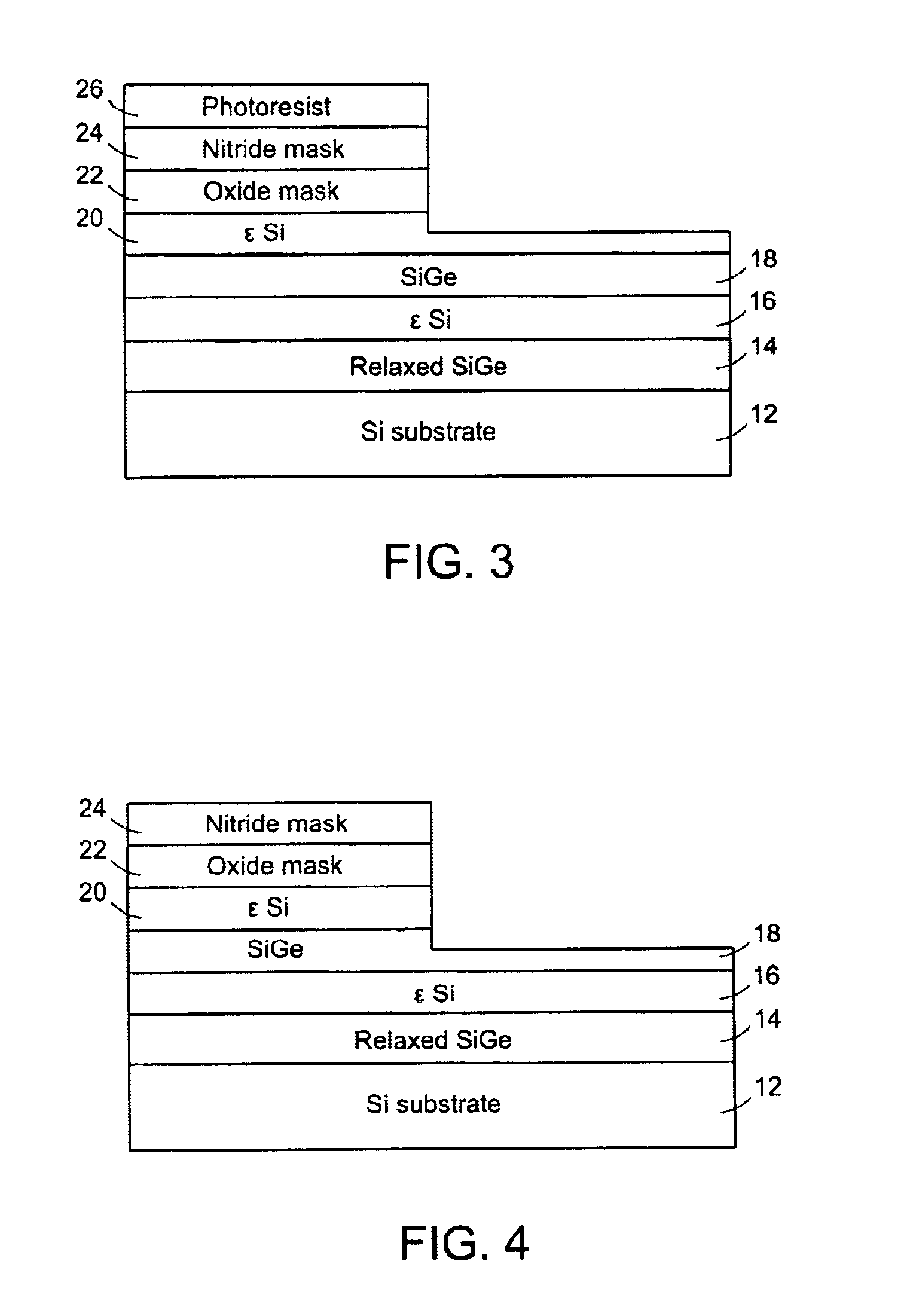
[0016]The invention provides a simplified method of forming buried and surface channel heterostructure devices on the same substrate. As aforementioned, conventional Si based integrated buried and surface channel devices are typically manufactured using complex implantation procedures. In the present invention, the starting substrate material defines the buried and surface channel device structures. This starting material is a heterostructure where the the different materials in the heterostructure have different oxidation or removal properties. The difference in material properties allows for the selective removal of particular layers and this allows for the integration of varied device structures.

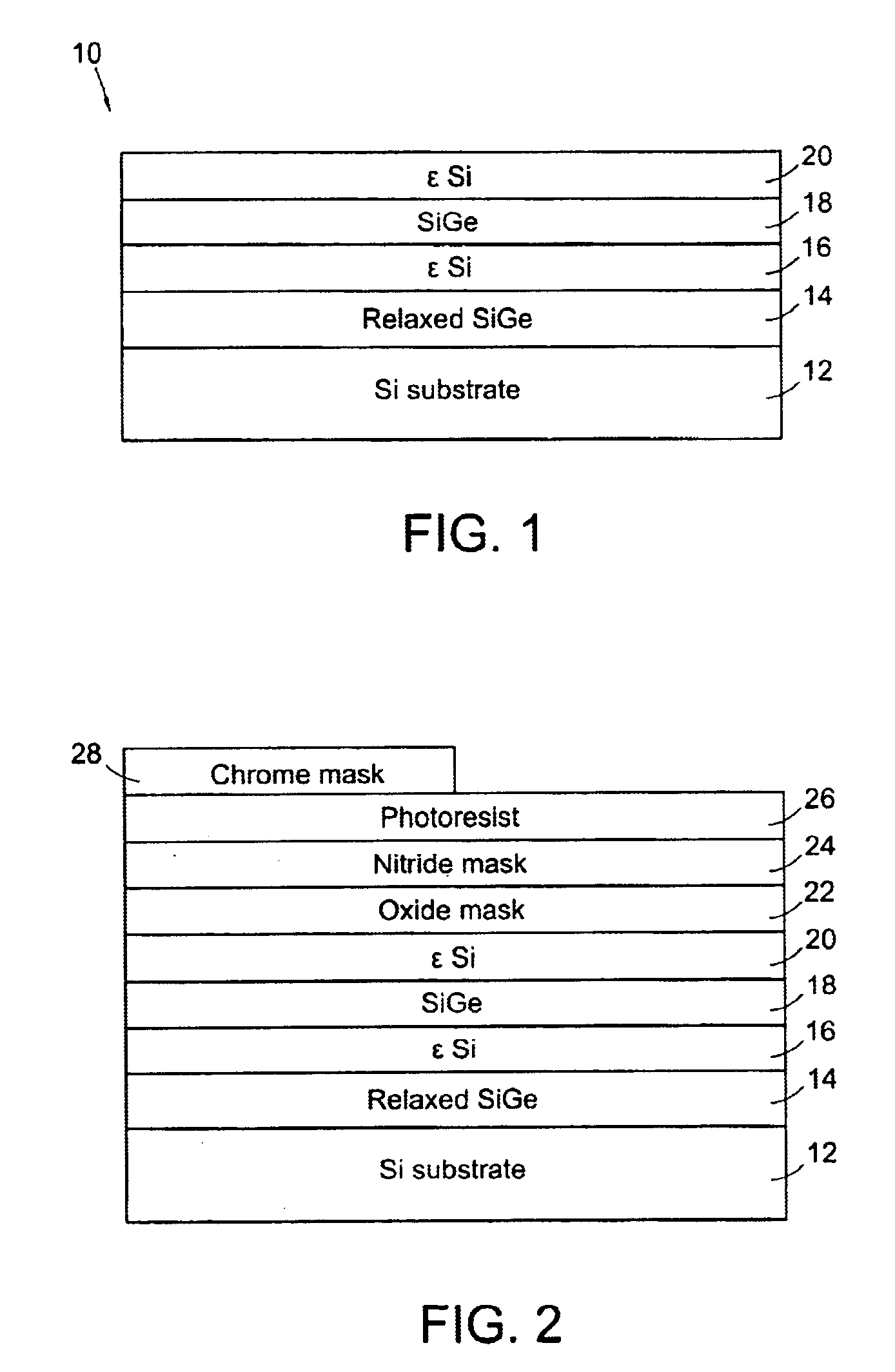
[0017]An exemplary embodiment of such a heterostructure substrate is a strained silicon substrate. A strained silicon (Si) substrate is generally formed by providing a relaxed SiGe layer on bulk Si through either epitaxial deposition or wafer bonding, and then providing a Si layer on the ...


PUM


Abstract

A method is disclosed of forming buried channel devices and surface channel devices on a heterostructure semiconductor substrate. In an embodiment, the method includes the steps of providing a structure including a first layer having a first oxidation rate disposed over a second layer having a second oxidation rate wherein the first oxidation rate is greater than the second oxidation rate, reacting said first layer to form a sacrificial layer, and removing said sacrificial layer to expose said second layer.

Description

[0001]The present application claims priority to U.S. Provisional Patent Application Ser. No. 60 / 298,153 filed Jun. 14, 2001.BACKGROUND OF TIE INVENTION[0002]The present invention generally relates to the fabrication of semiconductor substrates from devices, and in particular relates to the use of strained silicon (Si) heterostructure substrates in forming devices such as transistors, for example, for high-performance CMOS integrated circuit products.[0003]As microelectronic systems require faster operating speeds and increased computing power, the need exists for integrated circuits to provide a greater complexity of transistors in a smaller amount of circuit real estate. Such integrated circuits include, for example, microprocessors, ASICs, embedded controllers, and millions of transistors, such as metal oxide silicon semiconductor field-effect transistors (MOSFETs).[0004]Certain microelectronics systems, such as radars, satellites, and cell phones, require low-power, high-speed, ...

Claims


Application Information

Patent Timeline
Patent Type & Authority Patents(United States)
IPC IPC(8): H01L21/02H01L21/336H01L21/469H01L21/76H01L21/70H01L21/8242H01L21/31H01L21/8244H01L21/00H01L21/311H01L21/316H01L21/8238H01L29/10H01L29/78
CPCH01L21/823807H01L29/1054H01L29/7833
Inventor HAMMOND, RICHARDCURRIE, MATTHEW
Owner TAIWAN SEMICON MFG CO LTD
Why Eureka
Try Eureka